Video of the Day

Thursday, September 3, 2015

0

Simple Adjustable Staircase Waveform Generator

Staircase signals find many applications in the field of electronics, such as in television systems, telemetry, and analogue and digital communications. Here is a circuit illustrating the basic principles of staircase waveform generator. Advantages of this circuit are: simple, low-cost, no complex programming, easy-to-assemble on a breadboard and adjustable staircase waveform outputs of variable step sizes and durations.

Circuit and working
The circuit diagram of a simple adjustable staircase waveform generator is shown in Fig. 1.

IC1 (74HC14) is a hex inverter Schmitt trigger that generates oscillatory pulse (square wave) and gives an output clock at pin 14 of IC2 (74HC93), which is a 4-bit binary ripple counter. Pins 8, 9 and 12 of IC2 are connected to select pins of IC3 (74HC4051), which is an 8-channel analogue multiplexer/demultiplexer with three digital selected pins 9, 10 and 11. Input pins of IC3 are connected to eight potentiometers of 10-kilo-ohm each.


Variable step sizes are obtained by varying these potentiometers. Depending on the selected pins and values of potentiometers, we get different types of staircase waveforms at output pin 3 of IC3. When these waveforms are further given to the input pins of IC4 (dual op-amp), it simply buffers them. Fig. 2 shows four different types of staircase output waveforms obtained at CON5.

 Fig. 1: Circuit diagram of simple adjustable staircase waveform generator


Fig. 2: Staircase output waveforms

Vcc depends on the ICs used in the circuit and can be 5V. With CMOS ICs like 74Cxxx and CD4000B, we can use Vcc up to 15V.

Construction and testing
An actual-size, single-side PCB layout of the simple adjustable staircase waveform generator is shown in Fig. 3 and its component layout in Fig. 4.

The frequency at pins 1 and 2 of IC1 depends on the type of IC used and values of capacitors and resistors connected to gate N1 of the IC. It can be from 1Hz to 1MHz. If you use an external frequency, move S1 to position 5 to bypass capacitors C1 through C4.

Switch S2 selects the source of reference voltage for VR1 through VR8. In the first position (1), Vcc is used as reference source. In the second position (3), signal from connector CON3 is used as reference source.

Fig. 3: An actual-size PCB layout
   
 Fig. 4: Component layout of the PCB


The fixed-amplitude staircase output waveform is obtained at CON5 and variable-amplitude staircase waveform is obtained at CON6.


Each waveform consists of eight clock pulses, zero through seven. The height of each step is adjusted according to the need using potentiometers VR1 through VR8. The frequency of the step is determined by the oscillator around gate N1 of IC1 or by the external clock signal applied to connector CON1. For troubleshooting, check the various test points and ensure you get the outputs as per table.


Sourced by : EFY : Author Petre TZV Petrov


Sunday, August 16, 2015

0

Sequential Tilt-Motion Lock

Here is a project for locking and unlocking with a tilt sensor by tilting it in a defined sequence. It uses an accelerometer module to detect the tilt motion. If the sequence matches with the predefined motion sequence, the lock opens. You can build this lock for a briefcase, ballot box, portable cashbox or even as a door-lock using suitable mechanical arrangement.

Circuit and working
Fig. 1 shows circuit diagram of the sequential tilt-motion lock. The circuit is built around Arduino Uno board (Board1), accelerometer module (ACC.1), solenoid lock/electric strike and a few other components.

Circuit diagram of sequential tilt-motion lock
Fig. 1: Circuit diagram of sequential tilt-motion lock

Arduino Uno board. Arduino is an open source electronics prototyping platform based on flexible, easy-to-use hardware and software. It is intended for artists, designers, hobbyists and anyone interested in creating interactive objects or environments.
Arduino Uno is a board based on ATmega328 microcontroller. It consists of 14 digital input/output pins, six analogue inputs, a USB connection for programming the on-board microcontroller, power jack, an ICSP header and a reset button. It is operated with a 16MHz crystal oscillator and contains everything needed to support the microcontroller. It is very easy to use as the user simply needs to connect it to a computer with a USB cable, or power it with an AC-to-DC adaptor or battery to get started. The microcontroller on the board is programmed using Arduino programming language and Arduino development environment.

Pins A0, A1, A2, A3, A4 and A5 of Board1 are connected to pins ST, Z-axis, Y-axis, X-axis, GND and Vcc of the accelerometer module, respectively. Pin 10 of Board1 is connected to solenoid driver transistor through which the solenoid lock is connected.

Accelerometer module. An accelerometer is an electromechanical device that measures acceleration. The accelerometer module used here is based on ADXL335 triple-axis accelerometer from Analog Devices. The sensor has a full sensing range of ±3g.

The microcontroller in Board1 receives data at pins A1, A2 and A3 for z, y and x axes, respectively, from the accelerometer. This data is continuously compared by Board1 with predefined values for each axis. If the received sequence matches, Board1 unlocks the lock, which is either a solenoid lock or any other suitable magnetic lock. (We used a 12V electric strike for testing.) Glowing of LED1 indicates that the lock is open.

Software
The software for this project is written in Arduino programming language. The Arduino Uno is programmed using Arduino IDE software. ATmega328 on Arduino Uno comes with a boot loader that allows you to upload new code to it without the use of external hardware programmer. It communicates using the STK500 protocol. You can also bypass the boot loader and program the microcontroller through in-circuit serial programming (ICSP) header, but boot loader programming is quicker and easier. Select the correct board from ‘Tools → Board’ in Arduino IDE and burn the program (sketch) through standard USB port in the computer.

Fig. 2: An actual-size PCB layout for the sequential tilt-motion lock

Fig. 3: Component layout for the PCB


Construction and testing

An actual-size (Arduino shield type), single-side PCB for the sequential tilt-motion lock is shown in Fig. 2 and its component layout in Fig. 3. Assemble the circuit on the recommended PCB to minimize assembly errors.

To test the circuit for proper functioning, switch on S1 and verify correct 12V supply for the circuit at TP1 with respect to TP0.

The neutral position of accelerometer module is parallel to the earth’s surface. The +Y and +X axes are marked on the accelerometer module. The default tilt sequence of this circuit defined in the source code is -X, -Y, -X, +Y, -Y. If the tilt sequence is correct, you can observe the glowing of an in-built LED (not shown here) connected to pin 13 of Arduino board. If you want to change the sequence, change it in the source code, recompile the program and burn into the microcontroller.

To open the lock, switch on S1 and tilt the circuit sequentially, as mentioned above, within one minute. If correct action is not completed within one minute, you need to repeat the tilt sequence from the start to unlock it. To close the lock, just switch off the circuit using on/off switch S1.


Soueced By : EFY Author:  Akhil Kaushik


Saturday, August 8, 2015

0

12V, 1A SMPS Circuit Diagram

Most electronics enthusiasts require DC power supplies to operate various devices and accessories. The most popular and common supply is a 12V DC supply that can be easily derived from the household AC supply with transformation, rectification, filtering and stabilisation. These power supplies have a bulky steel- or iron-laminated transformer that provides a safety barrier for the low-voltage output from the AC input, and reduces the input from typically 230V AC to a much lower voltage. The low-voltage AC output from the transformer is then rectified by two or four diodes and smoothed into low-voltage DC by large electrolytic capacitors.


Fig. 1: The author’s prototype

A switched mode power supply (SMPS) offers the same end results at a lower cost and higher efficiency. For a given output power, an SMPS is lighter and smaller. This is because, if the frequency of operation is increased, one can get away with using a smaller core cross-sectional area. Besides, an iron-core transformer works only up to about 10 kHz, and if we need something in 50-100kHz range, we need a ferrite core.


Circuit and working

Fig. 2 shows the circuit of a simple 12V, 1A SMPS. The circuit is built around a low-power offline switcher TNY266 (IC1), photo-transistor photo-coupler EL817 (IC2), a flyback transformer (X1) and some other easily-available components.

Low-power offline switcher (TNY266). The SMPS here has been designed using a TNY266 chip, which is affectionately called the ‘555’ of SMPS. This device has a 700V power MOSFET, an oscillator, a high-voltage switched current source, a current limiting and thermal shutdown circuitry integrated onto a monolithic device. The start-up and operating power is derived directly from the voltage on the drain (pin 5), eliminating the need for a bias winding and associated circuitry. In addition, the device incorporates auto-restart, line under-voltage sense, and frequency jittering.

The drain-source breakdown voltage of the MOSFET in TNY266 is important. During the ‘off’ period, the MOSFET sees rectified 317V DC approximately. Additionally, it sees the reflected voltage of the secondary, which is about 130V AC. It also encounters the ringing voltage from the leakage inductance, and the drain-source capacitance of the MOSFET. Therefore a MOSFET with a Vdss of 650V DC is expected to keep the necessary safe operating margin. Fortunately, a MOSFET with these properties is included in TNY266.

The 230V AC input is connected at CON1, which is rectified by diode D1. The neon lamp (NL1) glows when the input supply is present. Resistor R1 limits the current through the lamp. The rectified output goes to the first terminal (A) of coil L1 and the second terminal (B) is connected to the drain of the inbuilt MOSFET in IC1. Diodes D2 and D3 are essentially the snubbers, and are used to protect the MOSFET from going above 600V.

Flyback transformer. A flyback circuit is simply a pair of coupled inductors. If a current is passed through one inductor, it will store energy E = ½ (L.I2), where ‘L’ stands for inductance in henry, and ‘I’ for current in amperes. This energy can later be taken out of the second inductor, which is coupled to the former at a different volt-current ratio. The flyback’s energy storage and extraction mechanism is interesting. The key point is the polarity of the winding; the secondary is out of phase with the primary, as is evident in Fig. 2 (the dots indicate polarity).

12V, 1A SMPS Circuit Diagram

Fig. 2: Circuit of the 12V, 1A SMPS


Fig. 3: An actual-size, single-side PCB for the 12V, 1A SMPS


Fig. 4: Component layout for the PCB

When the MOSFET of IC1 is ‘closed,’ the current flows through L1. Point A on L1 goes positive and by transformer action, and considering the polarity of dots, point C on L2 goes negative. This reverse biases diode D4, and no current flows in the secondary winding. Similarly, when the MOSFET is ‘open,’ the current flow through L1 is interrupted and, by Lenz’s Law, a voltage of polarity opposite to the applied voltage appears on L1 and L2. Thus, point A on L1 goes negative and point C on L2 goes positive. This situation forward biases diode D4. The energy stored in the core causes the current to flow through winding L2. This charges capacitor C2 and also powers the load. The charge on C2 is used in the next half of the cycle to keep the current through the load somewhat constant. The cycle repeats endlessly. The MOSFET is switched on/off continuously at a frequency of around 120 kHz to keep this process running.

The design data for the transformer is as follows:
1. Duty cycle = 0.45 (max. duty cycle for DCM flyback = 0.5; less 10% safety margin)
2. Core saturation magnetisation Bsat = 0.24T
3. Core area of EE20 = 25mm2

Winding details computed for the SMPS are shown in Table I.

The feedback circuit. Regulated output needs feedback to control the pulse width modulation (PWM) of the MOSFET. TNY266 has a fabulous control feature; it stops the switching cycle as soon as any current is taken out of pin 4 of the device. If SMPS output exceeds the zener break-down voltage then ZD1 conducts. This lights the opto-LED and the opto-transistor grounds pin 4 of IC1, resulting in immediate stoppage of the switching cycle. Also, when the primary is conducting, diode D4 on the secondary side is reverse biased. At this time, if the voltage across D4 exceeds its reverse breakdown voltage, the SMPS will fail. Here we have used an SB160 Schottky diode with breakdown voltage= 60V.

Connector CON2 provides 12V regulated DC supply.

Construction and testing
A general core-selection ‘rule of thumb’ for SMPS below 50 watts is 2-3 mm2 core area per watt. For a primary input power of 16W, a core with a core area of 32-48 mm2 is needed. EE20 core will work well for this design.

Transformer wire. Any wire that can carry the required current can be used. To know how much current a given wire can carry, SMPS designers use a number called current density [J] for this calculation. Empirically, a good starting point is J = 5 amps/mm2. The primary carries 0.3 amps, so it can be wound using SWG 38. The secondary carries 5 amps, so it can be wound with SWG 26. A good practice would be to wind the secondary using two parallel strands of SWG 28. This reduces the skin effect. The key problem in flyback transformers is leakage inductance, which is caused by poor coupling between the primary and secondary windings. So wind them tight, with full overlap.

The air gap. Flybacks made from power ferrites must have an air gap. The energy stored in a flyback primary is E = ½ L.I2. Peak primary current depends inversely on primary inductance. An air gap increases the energy storage capacity of a flyback transformer. It is calculated as follows:
Air gap = (µ0 x N2 x Ac)/Lprimary
where:
µ0 = permeability of free space, 4π x 10-7
Ac = Core area (m2)
N = Primary turns
Lprimary = (Vprimary.pk × Ton.primary)/ Iprimary.pk

The primary inductance computes to ~3mH, so the air gap is approximately 0.2mm. However, this value is not critical, as was experienced by the authors during their experiments. Any air gap in the neighbourhood of the calculated value works well. A thin sheet of plastic or paper works fine.

An actual-size, single-side PCB for the simple 12V, 1A SMPS is shown in Fig. 3 and its component layout is shown in Fig. 4. Assemble the circuit on the recommended PCB to minimise assembly errors. Use IC base for IC1.

To test if the circuit is functioning properly, first check the regulated output at TP1 with respect to TP0. The voltage should be stable with or without a load.


Sourced By: EFY Author : AshvinI Vishvakarma and Atanu Dasgupta


Saturday, July 18, 2015

0

Footstep Power Generation System using Microcontroller

Day by day, the population of the country increased and the requirement of the power is also increased. At the same time the wastage of energy also increased in many ways. So reforming this energy back to usable form is the major solution. As technology is developed and the use of gadgets, electronic devices also increased. Power generation using conservative methods becoming deficient. There is a necessity arises for a different power generation method. At the same time the energy is wasted due to human locomotion and many ways. To overcome this problem, the energy wastage can be converted to usable form using the piezoelectric sensor. This sensor converts the pressure on it to a voltage. So by using this energy saving method, that is the footstep power generation system we are generating power.

Footstep Power Generation System using Microcontroller

Microcontroller based Footstep Power Generation System


This project is used to generate voltage using footstep force. The proposed system works as a medium to generate power using force. This project is very useful in public places like bus stands, theaters, railway stations, shopping malls, etc. So, these systems are placed in public places where people walk and they have to travel on this system to get through the entrance or exists. Link


0

Hovercraft Controlled By Android

A hovercraft is a non wheeled vehicle that can hover over land as well as water easily using high powered fans and aerodynamic design. We here propose an advanced hovercraft that uses high rpm motors interfaced with an avr family microntroller to achieve desired functionality. The motor below hovercraft rotates at a very high RPM that allows it to generate a force enough to make it hover on the surface thus reducing the friction below it to minimum. Then we use the motor propeller mounted behind it to push the hovercraft in forward direction. Now we also need to use a servo motor attached to the hovercraft rudder that helps the hovercraft to move in desired directions by bending the air at accurate angles. 

Hovercraft Controlled By Android


The system works collectively to hover while continuously managing servo as well as propeller motor to drive the hovercraft as desired. Now to control the hovercraft we here use an android application. The android application sends movement commands to the hovercraft circuit. The circuit consists of an Bluetooth receiver to receive and process these commands. The commands received by receiver are now processed by the microcontroller and it then operates all three motors accordingly as desired by the user. Link


Monday, July 13, 2015

0

Versatile Audio-Visual Alarm Circuit Diagram

This circuit uses an NE555 timer IC, some LEDs, a couple of piezo buzzers and a few other components to produce audio-visual effects as per your requirement. The timer NE555 and its equivalents are widely used for all sorts of audio and visual indications, such as door alarms. But the sound produced by these circuits may not be always pleasant to hear, or the light produced may not be visually appealing. With this circuit you can get different audio-visual effects.

Here we use LEDs for visual indication and buzzers for audible alarms as they require relatively low current to operate. By simply connecting some resistors and capacitors to NE555 we can obtain some interesting visual and audible effects as described here.

Circuit and working
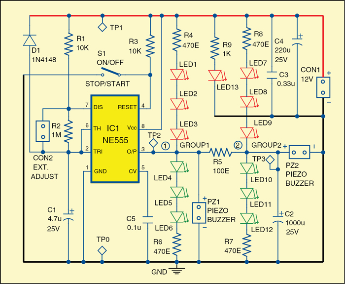
Fig. 1 shows the circuit of the versatile audio-visual alarm which is built around timer NE555 (IC1), LEDs, buzzers and some resistors and capacitors. Resistors R1 and R2 and capacitor C1 determine the frequency of the LEDs’ blinking. The frequency is selected usually within the range of 0.1Hz to 20Hz, depending on your requirement. Values of resistors R1 and R2 can be above 1-kilo-ohm. Capacitor C1’s value can be between 1µF and 1000µF.


Versatile Audio-Visual Alarm Circuit Diagram
Fig. 1: The versatile audio-visual alarm circuit


Fig. 2: Actual-size, single-side PCB for the circuit
  
Fig. 3: Component layout for the PCB


Timer NE555 drives two outputs, namely, Group1 and Group2. Group1 is built around resistors R4 and R6 along with LED1 through LED6. Group2 is built around resistors R7 and R8 along with LED7 through LED12.


Each of the groups can be configured to get different outputs. For example, in Group1 you can use only the LEDs (LED1 through LED3) connected to +12V, or only the LEDs (LED4 through LED6) connected to the ground, or both branches of these LEDs, or only piezo buzzer PZ1, or PZ1 with any combination of the LEDs, or you can omit the entire Group1.

The components in Group2 can form the same combinations as the components in Group1. The difference between the Group1 and Group2 is the use of resistor R5 and capacitor C2. These two components give light-decay effect to the LEDs and a pleasant low-pitch sound to piezo buzzer in Group2. Value of resistor R5 can be between 75-ohm and 1-kilo-ohm and that of capacitor C2 between 47µF and 1000µF.

At point 1 (TP2) in the circuit you can see a rectangular wave signal. At point 2 you can see a triangular or trapezoidal-like signal. The signals at points 1 and 2 should go low, almost to zero, and should go high, almost to 12V supply voltage.

Power supply used is 12V, but it can be in the range of 4.5V to 15V as well, depending on the number of LEDs used in each branch. Higher number of LEDs will require higher voltage. LED13 glows when power supply is connected in the circuit.

Resistors R4, R6, R7 and R8 are selected according to the number and type of the LEDs used. If the values of these resistors are too low, the output of the timer will be overloaded and the LEDs in the upper and the lower branches will get activated simultaneously.
 
Overloading may also damage the NE555 timer. It is suggested to keep the total output current drawn from NE555 below 100mA.

On/off switch S1 is used to start or stop the alarm. Connector CON2 is an optional input point for connecting a variable element, such as a preset, for adjusting or varying the frequency of the square signal for more audio-visual effects.

Construction and testing
An actual-size, single-side PCB for the versatile audio-visual alarm is shown in Fig. 2 and its component layout in Fig. 3. After assembling the circuit on PCB, enclose it in a suitable plastic box.

Connect piezo buzzers PZ1 and PZ2 at their provided places in the PCB. Also connect 2-pin terminal CON1 for power supply. Connect CON2 for external input (optional). Before using the alarm circuit, check at the test points given in the table.


Sourced By: EFY Author:  Petre Tzv Petrov


Wednesday, July 8, 2015

0

Power 2h-30-Vatt 12 volts, working scheme

Not expensive, High-quality sound, Small parts and easy to assemble, Do not need to be tuned.Today can offer to your attention an amplifier that I have gathered from (almost) stuff I have lying in store. Long ago, working in the workshop, we often filmed amplifiers machines, since they come without tape recorders ​​and to put an ordinary tape recorder had to dismantle the amplifiers are !!! I left a couple of times since amplifier chips such as the LA4708. Time has passed since then a lot until my sister had not asked to do anything for his laptop to play in the yard with an acceptable quality and loud sound as speakers 2 pcs idle at home!


Power 2h-30-Vatt 12 volts, working scheme


 Power 2h-30-Vatt 12 volts, working scheme


It is taken from the datasheet half and half just from the people and schemes are proven over the years !!! If you look at the diagram, the capacitors C3 and C4 - a savings standing on the output of the amplifier, without a way (as if the sound disappears at high bass and not enough to drive the speakers). The amplifier where I desoldering the chip standing at the entrance storage choke (but I was too lazy to shake it, because it was a little too big standard, and the image at the top of his nebylo), it was decided to do without it !!! Increased denomination was in microfarads and capacitor C7 to 3300 microfarads, put dop.kondensatory input to the sound source and of the zener instead I put krenochku 5V to 5 foot (because it was under the hand) Well, all of the components that we need:


Sorry I forgot to add a couple of SMD capacitors there, standing at the entrance, but roughly the size of clear =) I must say that the capacitors C1, C2, C5, C6 (Mylar or polypropylene). Next Ludim, drills, soldered components from small to large. Unfortunately I lost zaglyuchila feshka and photos with my tinning and soldering = (There was only the result of the test and for 2 weeks =)

Put it on the active cooling, in Signet will be provided !!! My advice is not to actively, but rather to increase the area of the radiator. The following seals:


Power gives its net 20-30 watt channel! Tested on AS35! Keep in mind that this , no volume controls are not present !!! Before starting up the volume to a minimum !!! Starts amplifier from normal BP computer, it still works as well (there is no time to stick his body =)


Thursday, July 2, 2015

0

Simple Mini Offline UPS Circuit Diagram

Most of the systems are powered by AC mains. Uninterrupted power supply systems (UPSes) are there as a back-up to power the systems when mains supply is interrupted due to a power cut. A UPS differs from a standby generator in that it will provide near-instantaneous power by supplying the energy stored in batteries. In an online UPS, batteries are always connected to the inverter, which is always on, so that no transfer switches are necessary when power disruption occurs.

In an offline UPS, the inverter circuit is switched on when mains are not there. UPSes are available off-the-shelf, and one can select the system as per one’s requirement, back-up time being one requirement. However, one can construct a UPS of one’s own choice. Here is a circuit of an offline UPS, which a hobbyist can make at a reasonable cost. The capacity of the UPS is 350VA, so it can be used for any equipment with a load below 350VA. The UPS can be upgraded to 1kVA by making just a few changes.

Circuit and working
The circuit diagram of the mini offline UPS shown in Fig. 1 has the following four sections:
Section 1: Mains/inverter change-over section
Section 2: Inverter section
Section 3: Battery-status-indicator section
Section 4: Oscillator section

Above-mentioned sections and their interconnections are appropriately marked in the circuit diagram.

Mains/inverter changeover section. The circuit of this section is built around step-down transformer X1 (230V AC primary to 12V-0-12V, 500mA secondary), a 12V DC, 3C/O (changeover) relay (RL1) and a few other components. 230V AC mains is connected to the circuit through connector CON7. Output of the UPS is available at connector CON8, which is actually a 3-pin socket.

Mains voltage is rectified by diodes D1-D2 (1N4007). The full-wave rectified output is smoothened by capacitor C1. DC voltage so generated is applied at pins 10 and 11 of relay RL1. When mains voltage is there, the relay gets energised to affect the changeover to connect the mains to the output of the UPS.


The circuit is not on a PCB and has been wired externally. Relay contacts in the circuit diagram are shown in a de-energised state of the relay.

Inverter section. This section comprises transformer X2, npn power transistors 2N3055 (T1 through T8) and power diodes 1N5407 (D3-D4). Transistors, which are eight in number, are connected in two banks. The number of transistors per bank will depend on the required VA rating. The prototype has been made for 350VA rating by using four transistors per bank. The number of transistors required per bank for different capacities are:
  • 550VA – Five
  • 650VA – Six
  • 1000VA – Seven

Simple Mini Offline UPS Circuit Diagram

Fig. 1: Circuit diagram of the mini UPS

This circuit is also not on a PCB and has been wired externally. Transistors T1 through T8 have been fitted on the same heat-sink. Mounting of transistors has to be done in such a manner that their base and emitter are not in contact with the heat-sink. The metal body of the transistor is the collector. Collectors should be separated from the heat-sink. This is done by using mica separators between the heat-sink and metal body of the transistor. In short, all three terminals should be separated from the heat-sink. The arrangement is shown in Fig. 2.

Interconnections of transistor terminals, transformer X2, diodes D3-D4, battery-status-indicator section and oscillator section are shown in a combined circuit diagram (Fig. 1). The heat-sink should also be isolated from the UPS box.


Fig. 2: Mounting of transistor 2N3055 on heat-sink
  
 Fig. 3: Details of the 3C/O relay

Fig. 4: PCB of the oscillator and the battery-status section


Fig. 5: Components of the PCB

Battery-status-indicator section. This section monitors the state of the battery. It is connected to the battery by CON3-CON4 combination. Connect these as per polarity of the 12V battery. Overcharge status of 14.4V is set with the help of preset VR3. Overcharge status is indicated by LED2.

We have to switch off S1 to protect the battery from overcharging. During normal charging, no LED (LED1 or LED2) will glow. If S1 is off, the rectifier circuit formed by diodes D3 and D4 will be disabled, which, in turn, will stop further charging of the battery. Lower limit of the battery is set at 11.3V with the help of preset low level of the battery, which will be indicated by LED1. Switch S1 has to be closed to restart the charging of the battery. Load should be disconnected when battery voltage is lower than 11.3V and mains voltage is not there.

Oscillator section. This circuit comes into action when mains voltage is not there. It, along with two banks of transistors T1-T8, will generate low-level AC voltage (15V-0-15V) at terminals of transformer X2, which will be stepped up by transformer X2.

The circuit is built around NE555 timer (IC2), dual JK flip-flop 4027 (IC1), transistors SK100 (T11-T12) and BC547 (T9-T10), voltage regulator 7805 (IC3) and a few other components. NE555 timer is configured in astable multivibrator mode.

Frequency of the timer is set to around 200Hz with the help of preset VR1 in order to get around 50Hz line frequency at CON1. Output of the timer from its pin 3 is fed to pin 3 (CP2) of second flip-flop of IC1 as clock pulse. Output of this flip-flop from pin 1 (Q2) is used to clock the first flip-flop. Outputs Q1 and Q1 are applied to the bases of transistors T9 and T10, respectively. Transistors T11 and T12 amplify these outputs to about 2.2V, which are applied to base terminals of transistors T4 and T8 for further amplification to 12V. Con1 and Con2 are used to connect outputs from the oscillator section to the two transistor banks.

The circuit is powered by a regulated 5V DC provided by voltage regulator 7805. Input to the regulator is the battery voltage, which we get by connecting Con5 to Con6. Battery voltage reaches pin 1 of regulator through pin 9 and pin 3 of relay RL1 and switch S2 is closed. When mains voltage is present, pin 9 and pin 3 are disconnected due to activation of the relay. Power supply to the oscillator section is interrupted, resulting in deactivation of the inverter circuit.

Relay RL1
Relay RL1 affects the necessary changeover required in the system due to the presence or non-presence of mains voltage. It is a 12V, three contacts changeover (three-poles  double-throw) relay. The arrangement of poles and contacts is shown in Fig. 3.

The coil of the relay is between terminals 10 and 11. Terminals 7 and 8 are shorted. Connections of remaining terminals of the relay are shown in circuit diagram (Fig. 1).

Working of the circuit
The UPS works in two modes:
1. When AC power is present
2. When AC power is absent

When AC power is present. When AC mains power is present, transformer X1 gets 230V AC input mains supply. Relay RL1 is therefore energised. Terminals 7, 8 and 9 of the relay come into contact with terminals 4, 5 and 6, respectively. Phase of the incoming AC mains supply gets connected to terminals 4, 7, 5 and 8 of the relay and the output socket where we connect the load. In this manner, mains are transferred to output socket CON8 of the UPS.


Fig. 6: The final assemblage enclosed in a cabinet (front panel)
  
 Fig. 7: The final assemblage enclosed in a cabinet (internal wiring)

When switch S1 is closed, the phase of the input mains gets connected to 230V tapping of transformer X2 through terminal 5 as it is in contact with the terminal 8 of the relay. As the neutral connection is common, transformer X2 acts as a step-down transformer. 230V AC is stepped down to 15V-0-15V AC and rectified to DC voltage by a full-wave rectifier (diodes D3-D4). Capacitor C7 is connected across the center tap of transformer X2. It is not included in the PCB. It is recommended to use a current limitter (say 4.7-ohm, 20W resistor) in series with positive terminal of the battery using suitable arrangement. The value of this current limitter will depend on your requirement, so it is not shown in the circuit here.

DC voltage so generated is used to charge the battery. At the same time, terminal 9 of the relay comes into contact with terminal 6, which disconnects power supply to the oscillator circuit and deactivates the inverter circuit. Switch S1 should be open when the battery is fully charged, which will be indicated by lighting up of LED2.

When AC mains power is absent(power cut). When AC mains power is off, transformer X1 does not get 230V AC supply. Relay RL1 therefore does not energise. Terminals 7, 8 and 9 of the relay come into contact with terminals 1, 2 and 3, respectively. Terminal 9 is connected to the positive terminal of the 12V battery, which is extended to the oscillator circuit. Inverter circuit comes into action.

Transformer X2 is now a step-up transformer. AC voltage from 240V tap of transformer X2 is connected to terminal 1 of the relay. As terminals 7 and 8 are in contact with terminals 1 and 2 of the relay, 240V AC gets connected to output socket CON8. Neon lamp N1 is connected between terminal 2 and neutral. It glows when the UPS is on. The output is connected to 240V tapping because there will be a voltage drop when load is connected to the UPS.

Construction and testing
Combined actual-size, single-side PCB for the oscillator section and the battery-status section is shown in Fig. 4 and the component layout in Fig. 5.

If needed, the PCB can be cut into two portions along the dotted line and mounted separately. Rest of the circuit has been wired using connectors. The final assemblage of the mini offline UPS is enclosed in a cabinet as shown in Fig. 6. The internal wiring is shown in Fig. 7 and the rear panel is shown in Fig. 8. All switches, indicators and terminals for connecting the battery and output socket are to be placed aesthetically on the front panel of the cabinet.


Fig. 8: The final assemblage enclosed in a cabinet (rear panel)

Fuse F1 (1A) is used to protect the device from any short circuits. All connections should be made very carefully. The load should not exceed 350VA. For troubleshooting, check voltages at various test points as listed in the table.

Caution. Please be careful as the circuit operates on 230V AC.


Sourced By: EFy Author:  ZameerudDin Syed


Monday, June 29, 2015

0

Simple Versatile Audio-Visual Alarm Circuit Diagram

This circuit uses an NE555 timer IC, some LEDs, a couple of piezo buzzers and a few other components to produce audio-visual effects as per your requirement. The timer NE555 and its equivalents are widely used for all sorts of audio and visual indications, such as door alarms. But the sound produced by these circuits may not be always pleasant to hear, or the light produced may not be visually appealing. With this circuit you can get different audio-visual effects.

Here we use LEDs for visual indication and buzzers for audible alarms as they require relatively low current to operate. By simply connecting some resistors and capacitors to NE555 we can obtain some interesting visual and audible effects as described here.

Circuit and working
Fig. 1 shows the circuit of the versatile audio-visual alarm which is built around timer NE555 (IC1), LEDs, buzzers and some resistors and capacitors. Resistors R1 and R2 and capacitor C1 determine the frequency of the LEDs’ blinking. The frequency is selected usually within the range of 0.1Hz to 20Hz, depending on your requirement. Values of resistors R1 and R2 can be above 1-kilo-ohm. Capacitor C1’s value can be between 1µF and 1000µF.

Simple Versatile Audio-Visual Alarm Circuit Diagram


Simple Versatile Audio-Visual Alarm Circuit Diagram

Fig. 1: The versatile audio-visual alarm circuit


Fig. 2: Actual-size, single-side PCB for the circuit
  
 Fig. 3: Component layout for the PCB

Timer NE555 drives two outputs, namely, Group1 and Group2. Group1 is built around resistors R4 and R6 along with LED1 through LED6. Group2 is built around resistors R7 and R8 along with LED7 through LED12.


Each of the groups can be configured to get different outputs. For example, in Group1 you can use only the LEDs (LED1 through LED3) connected to +12V, or only the LEDs (LED4 through LED6) connected to the ground, or both branches of these LEDs, or only piezo buzzer PZ1, or PZ1 with any combination of the LEDs, or you can omit the entire Group1.

The components in Group2 can form the same combinations as the components in Group1. The difference between the Group1 and Group2 is the use of resistor R5 and capacitor C2. These two components give light-decay effect to the LEDs and a pleasant low-pitch sound to piezo buzzer in Group2. Value of resistor R5 can be between 75-ohm and 1-kilo-ohm and that of capacitor C2 between 47µF and 1000µF.

At point 1 (TP2) in the circuit you can see a rectangular wave signal. At point 2 you can see a triangular or trapezoidal-like signal. The signals at points 1 and 2 should go low, almost to zero, and should go high, almost to 12V supply voltage.

Power supply used is 12V, but it can be in the range of 4.5V to 15V as well, depending on the number of LEDs used in each branch. Higher number of LEDs will require higher voltage. LED13 glows when power supply is connected in the circuit.

Resistors R4, R6, R7 and R8 are selected according to the number and type of the LEDs used. If the values of these resistors are too low, the output of the timer will be overloaded and the LEDs in the upper and the lower branches will get activated simultaneously.

Overloading may also damage the NE555 timer. It is suggested to keep the total output current drawn from NE555 below 100mA.

On/off switch S1 is used to start or stop the alarm. Connector CON2 is an optional input point for connecting a variable element, such as a preset, for adjusting or varying the frequency of the square signal for more audio-visual effects.

Construction and testing
An actual-size, single-side PCB for the versatile audio-visual alarm is shown in Fig. 2 and its component layout in Fig. 3. After assembling the circuit on PCB, enclose it in a suitable plastic box.

Connect piezo buzzers PZ1 and PZ2 at their provided places in the PCB. Also connect 2-pin terminal CON1 for power supply. Connect CON2 for external input (optional). Before using the alarm circuit, check at the test points given in the table.


Sourced By: EFY Author :  Petre Tzv Petrov


Monday, June 15, 2015

0

Audio Compressor circuit components Liabilities

We have seen here on the blog a very interesting audio compressor circuit, the audio compression is the process that adjusts the level of an audio signal, reducing the volume of loud sounds or amplifying low sounds by narrowing or dynamic range compression an audio signal.

The audio compression is used for sound recording, playback, radio and amplifiers for musical instruments, among other utilities. This circuit presented here is a single audio compressor that uses only passive components, or any semiconductor such as transistor, diode or integrated circuit.


Audio Compressor circuit


Audio Compressor circuit components Liabilities


This compressor dynamic audio with passive components reduces the high signal to a lower signal, but more constant. If you look at this circuit will realize that has no power supply because it only reduces the input signal.

The basic operation is simple in its exit from the compressor will have a constant audio signal of approximately 70mV, so when the input voltage is between 100mV and 10Volts. The reduction control is made by the variable resistor P1 which may be a potentiometer or trimpot.

The diodes of this circuit should be germanium, because this type of diode has limits below the forward bias silicon diodes. Despite being simple this compressor circuit should work well, the drawback is its great attenuation, which makes it unfeasible for most audio applications.


Friday, June 5, 2015

0

Simple Motor Bike Brake Horn Circuit Diagram

The circuit can be operated from 4.5V to 12V DC or direct from the brake point of the motor-bike, Resistor R7 should be replaced with 1-ohm. 1/2W in case of an 8-ohm speaker. T5 is a driver transistor. C3 polarity can be reversed for a sudden off of the circuit.

Simple Motor Bike Brake Horn Circuit Diagram


Simple Motor Bike Brake Horn Circuit Diagram


PARTS LIST
Resistors (all ¼-watt, ~+mn~ 5% Carbon)
R1, R7 = 2.2 KΩ
R2, R4 = 820 Ω
R3, R5 = 470 Ω
R6 = 4.7 KΩ
R8 = 10 KΩ
R9 = 4.7 Ω, 0.5W

Capacitors
C1 = 22 µF/25v
C2 = 4.7 µF/63V
C3 = 100v/16V
C4 = 0.047 µF
C5 = 0.01 µF

Semiconductors
T1 – T4 = BC148B
T5 = SL100
Miscellaneous
LS1 = 4Ω speaker


Thursday, May 28, 2015

0

Low-Cost 6-Bit DAC Circuit Diagram

For controlling the load of appliances such as cooling fans, low-wattage heaters, thermostats, low-wattage light sources, small electrical toys and test benches for loudspeakers, we need a power source whose voltage can be controlled in small steps and is capable of providing current of more than 1A. For that, we require low-resolution digital-to-analogue converters (DACs) with three to seven bits.

Here is the circuit capable of setting output voltage between 1.25V and 15V in 64 steps. The circuit can be adapted for a lot of applications.

Low-Cost 6-Bit DAC Circuit Diagram
 Low-Cost 6-Bit DAC Circuit Diagram

Circuit and working

The circuit of the low-cost 6-bit DAC is shown in Fig. 1. The DAC is built around IC 7406, hex inverter (IC3). We may also use IC 7407 with six followers without changing the PCB. Steps are generated with the help of 6-bit digital input code D0 (LSB) through D5 (MSB) at CON2. Consequently, 64 combinations are possible starting from 000000 to 111111. At each combination, you will have a pre-determined output voltage between 1.25V and the possible maximum 15V.
Inputs D0 through D5 are TTL and CMOS compatible. These can be generated by microcontrollers, parallel-interface adapters such as PPI8255A, PIA6820/1 and Z80-PIO. In the simplest case, inputs can be driven with switches connecting inputs D0 through D5 to ground 0V or to 5V.

The size of the steps is programmable with trimmer potentiometers VR1 through VR6. Consequently, we can produce regular or irregular steps according to the need, depending on the characteristics of the load being controlled.

You can set any output voltage with any potentiometer between 1.25V and the maximum. For example, if you have a transformer for 18V AC, you can set outputs between 1.25V and around 15V with any potentiometer.

For adjustment in the simplest case, apply a set of seven test codes, as listed below, on CON2; output on CON3 will be as under.

Test code with 7406 (invert with 7407):
000000 Vout=Vmax (unadjustable)
000001 Vout=1.25V (VR1)
000010 Vout=3V (VR2)
000100 Vout=5V (VR3)
001000 Vout=7.5V (VR4)
010000 Vout=9V (VR5)
100000 Vout=12V (VR6)

The maximum output voltage on CON3 and CON4 is with code 111111 on the outputs of IC3 and depends on the input voltage of IC2. Please note that, if you use 7407, the codes will be non-inverted, and if you use 7406, the codes will be inverted.

The 6-bit input digital code D0 through D5 is buffered with 7406 or similar (IC3). With an open collector, the IC works as a translator/buffer between standard TTL levels to higher voltages needed for LM317.

Fig. 2: An actual-size PCB layout of the low-cost 6-bit DAC

Fig. 3: Component layout of the PCB

If the requirement of current is more than 1A, then select adjustable regulator IC2 from series LM317T (1.5A), LM350 (3A) or any compatible adjustable-linear regulator.

This makes the DAC adaptable to a lot of applications. In many cases, there is no need to start the output voltage from 0V. This makes the solution even simpler.

Input digital code D0 through D5 is buffered with IC3, which should be obligatory with open connector. The preferred device is 7406 or better, with outputs that can work with up to 30V.

Power requirements are from a common configuration built around step-down transformer X1 (secondary voltage 18V to 20V with current 1A or above), bridge rectifier BR1 and voltage regulator IC 7805 (IC1). The mains power is applied on connector CON1. 5V is available at connector CON5.

The selection of mains transformer X1, bridge rectifier and heat sinks for IC1 and IC2 depends on the required maximum output current from the DAC. IC1 and IC2 can be mounted on a common heat-sink after proper mounting is done.

The load is connected to connector CON3. A DC voltmeter with 50V range is connected at CON4 for measuring the output voltage. The DAC can be tested with 12V/5W/0.4A light bulb, 12V/0.3A fan, heating element for thermostat with nominal current up to 0.3A and maximum current below 1A and similar loads.

Construction and testing
An actual-size, single-side PCB layout for the low-cost 6-bit DAC is shown in Fig. 2 and its component layout in Fig. 3.


Sourced By: EFY Author:  Petre TZV Petrov


Social Time

Google Plus
Follow Us
Pinterest
Follow Us

Subscribe to our newsletter

(Get fresh updates in your inbox. Unsubscribe at anytime)