Video of the Day

Showing posts with label Powers. Show all posts

Tuesday, June 20, 2017

0

Simple Bio-Feedback Circuit Diagram

Feed-back, means a reaction to a stimulus, I will explain, the concept is simple, but explanation is a bit troubled, bio-feedback is to electronically feed back a user through sound or Visual, it is possible to control your meditation state, causing the user to reach a pre-established state at any time.

Simple Bio-Feedback Circuit Diagram

Simple Bio-Feedback Circuit Diagram


With this circuit it is possible to feedback from consciously varying the resistance of the skin, even though the equipment helps, even so will require training for this.

In order to use the biofeedback, the user must remain at rest, preferably lying down, since physical activity and variations of the emotional state influence the resistance of the skin, regardless of our will or unconsciously.

The biofeedback electrodes should be attached to the ring finger and index finger by tape or tape, and the hand should be in a comfortable, stationary position.

How Bio-Feedback Works

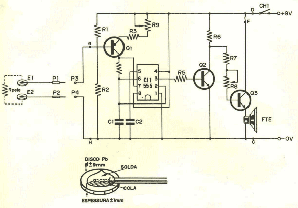
The biofeedback has as its main component an integrated circuit 555, configured as an astable multivibrator. The oscillation frequency of the 555 depends directly on the values of C1 and the collector current of Q1, which is connected as a current generator.

The resistors R1 and R2 attached to its base form a resistive divider which together with R3 and R9 determine the collector current of the transistor.

When the person connects the electrodes, the skin resistance is placed in parallel with R2, which changes the frequency of the oscillator. If skin resistance increases or decreases, we will see a drop or increase in the oscillation frequency of Cl1. R8 functions as volume control for Q3, which is the power amplifier.

Relation of Bio-Feedback Components

R1 – 47 kOhm x 1/4 Watt
R2 – 680 kOhm x 1/4 Watt
R3, R4, R6 – 1 kOhm x1/4 Watt
R5 – 22 kOhm x 1/4 Watt
R7 – 10 kOhm x 1/4 Watt
R8 – 50 kOhm – potentiometer linear
R9 – 10 kOhm – trimpot
C1 – 100 ηF pollster
C2 – 10 ηF pollster
CI1 – NE 555 ou equivalent
Q1 – BC 178 ou equivalent
Q2 – BC 549 ou equivalent
Q3 – 2N3055 ou equivalent
The biofeedback power is provided by a 9 Volt battery, but a well filtered source to avoid noise can be used without problems.
Source New Electronic Magazine 1 of 1977 - author of Gary Gronich.


Thursday, September 3, 2015

0

Simple Adjustable Staircase Waveform Generator

Staircase signals find many applications in the field of electronics, such as in television systems, telemetry, and analogue and digital communications. Here is a circuit illustrating the basic principles of staircase waveform generator. Advantages of this circuit are: simple, low-cost, no complex programming, easy-to-assemble on a breadboard and adjustable staircase waveform outputs of variable step sizes and durations.

Circuit and working
The circuit diagram of a simple adjustable staircase waveform generator is shown in Fig. 1.

IC1 (74HC14) is a hex inverter Schmitt trigger that generates oscillatory pulse (square wave) and gives an output clock at pin 14 of IC2 (74HC93), which is a 4-bit binary ripple counter. Pins 8, 9 and 12 of IC2 are connected to select pins of IC3 (74HC4051), which is an 8-channel analogue multiplexer/demultiplexer with three digital selected pins 9, 10 and 11. Input pins of IC3 are connected to eight potentiometers of 10-kilo-ohm each.


Variable step sizes are obtained by varying these potentiometers. Depending on the selected pins and values of potentiometers, we get different types of staircase waveforms at output pin 3 of IC3. When these waveforms are further given to the input pins of IC4 (dual op-amp), it simply buffers them. Fig. 2 shows four different types of staircase output waveforms obtained at CON5.

 Fig. 1: Circuit diagram of simple adjustable staircase waveform generator


Fig. 2: Staircase output waveforms

Vcc depends on the ICs used in the circuit and can be 5V. With CMOS ICs like 74Cxxx and CD4000B, we can use Vcc up to 15V.

Construction and testing
An actual-size, single-side PCB layout of the simple adjustable staircase waveform generator is shown in Fig. 3 and its component layout in Fig. 4.

The frequency at pins 1 and 2 of IC1 depends on the type of IC used and values of capacitors and resistors connected to gate N1 of the IC. It can be from 1Hz to 1MHz. If you use an external frequency, move S1 to position 5 to bypass capacitors C1 through C4.

Switch S2 selects the source of reference voltage for VR1 through VR8. In the first position (1), Vcc is used as reference source. In the second position (3), signal from connector CON3 is used as reference source.

Fig. 3: An actual-size PCB layout
   
 Fig. 4: Component layout of the PCB


The fixed-amplitude staircase output waveform is obtained at CON5 and variable-amplitude staircase waveform is obtained at CON6.


Each waveform consists of eight clock pulses, zero through seven. The height of each step is adjusted according to the need using potentiometers VR1 through VR8. The frequency of the step is determined by the oscillator around gate N1 of IC1 or by the external clock signal applied to connector CON1. For troubleshooting, check the various test points and ensure you get the outputs as per table.


Sourced by : EFY : Author Petre TZV Petrov


Saturday, August 8, 2015

0

12V, 1A SMPS Circuit Diagram

Most electronics enthusiasts require DC power supplies to operate various devices and accessories. The most popular and common supply is a 12V DC supply that can be easily derived from the household AC supply with transformation, rectification, filtering and stabilisation. These power supplies have a bulky steel- or iron-laminated transformer that provides a safety barrier for the low-voltage output from the AC input, and reduces the input from typically 230V AC to a much lower voltage. The low-voltage AC output from the transformer is then rectified by two or four diodes and smoothed into low-voltage DC by large electrolytic capacitors.


Fig. 1: The author’s prototype

A switched mode power supply (SMPS) offers the same end results at a lower cost and higher efficiency. For a given output power, an SMPS is lighter and smaller. This is because, if the frequency of operation is increased, one can get away with using a smaller core cross-sectional area. Besides, an iron-core transformer works only up to about 10 kHz, and if we need something in 50-100kHz range, we need a ferrite core.


Circuit and working

Fig. 2 shows the circuit of a simple 12V, 1A SMPS. The circuit is built around a low-power offline switcher TNY266 (IC1), photo-transistor photo-coupler EL817 (IC2), a flyback transformer (X1) and some other easily-available components.

Low-power offline switcher (TNY266). The SMPS here has been designed using a TNY266 chip, which is affectionately called the ‘555’ of SMPS. This device has a 700V power MOSFET, an oscillator, a high-voltage switched current source, a current limiting and thermal shutdown circuitry integrated onto a monolithic device. The start-up and operating power is derived directly from the voltage on the drain (pin 5), eliminating the need for a bias winding and associated circuitry. In addition, the device incorporates auto-restart, line under-voltage sense, and frequency jittering.

The drain-source breakdown voltage of the MOSFET in TNY266 is important. During the ‘off’ period, the MOSFET sees rectified 317V DC approximately. Additionally, it sees the reflected voltage of the secondary, which is about 130V AC. It also encounters the ringing voltage from the leakage inductance, and the drain-source capacitance of the MOSFET. Therefore a MOSFET with a Vdss of 650V DC is expected to keep the necessary safe operating margin. Fortunately, a MOSFET with these properties is included in TNY266.

The 230V AC input is connected at CON1, which is rectified by diode D1. The neon lamp (NL1) glows when the input supply is present. Resistor R1 limits the current through the lamp. The rectified output goes to the first terminal (A) of coil L1 and the second terminal (B) is connected to the drain of the inbuilt MOSFET in IC1. Diodes D2 and D3 are essentially the snubbers, and are used to protect the MOSFET from going above 600V.

Flyback transformer. A flyback circuit is simply a pair of coupled inductors. If a current is passed through one inductor, it will store energy E = ½ (L.I2), where ‘L’ stands for inductance in henry, and ‘I’ for current in amperes. This energy can later be taken out of the second inductor, which is coupled to the former at a different volt-current ratio. The flyback’s energy storage and extraction mechanism is interesting. The key point is the polarity of the winding; the secondary is out of phase with the primary, as is evident in Fig. 2 (the dots indicate polarity).

12V, 1A SMPS Circuit Diagram

Fig. 2: Circuit of the 12V, 1A SMPS


Fig. 3: An actual-size, single-side PCB for the 12V, 1A SMPS


Fig. 4: Component layout for the PCB

When the MOSFET of IC1 is ‘closed,’ the current flows through L1. Point A on L1 goes positive and by transformer action, and considering the polarity of dots, point C on L2 goes negative. This reverse biases diode D4, and no current flows in the secondary winding. Similarly, when the MOSFET is ‘open,’ the current flow through L1 is interrupted and, by Lenz’s Law, a voltage of polarity opposite to the applied voltage appears on L1 and L2. Thus, point A on L1 goes negative and point C on L2 goes positive. This situation forward biases diode D4. The energy stored in the core causes the current to flow through winding L2. This charges capacitor C2 and also powers the load. The charge on C2 is used in the next half of the cycle to keep the current through the load somewhat constant. The cycle repeats endlessly. The MOSFET is switched on/off continuously at a frequency of around 120 kHz to keep this process running.

The design data for the transformer is as follows:
1. Duty cycle = 0.45 (max. duty cycle for DCM flyback = 0.5; less 10% safety margin)
2. Core saturation magnetisation Bsat = 0.24T
3. Core area of EE20 = 25mm2

Winding details computed for the SMPS are shown in Table I.

The feedback circuit. Regulated output needs feedback to control the pulse width modulation (PWM) of the MOSFET. TNY266 has a fabulous control feature; it stops the switching cycle as soon as any current is taken out of pin 4 of the device. If SMPS output exceeds the zener break-down voltage then ZD1 conducts. This lights the opto-LED and the opto-transistor grounds pin 4 of IC1, resulting in immediate stoppage of the switching cycle. Also, when the primary is conducting, diode D4 on the secondary side is reverse biased. At this time, if the voltage across D4 exceeds its reverse breakdown voltage, the SMPS will fail. Here we have used an SB160 Schottky diode with breakdown voltage= 60V.

Connector CON2 provides 12V regulated DC supply.

Construction and testing
A general core-selection ‘rule of thumb’ for SMPS below 50 watts is 2-3 mm2 core area per watt. For a primary input power of 16W, a core with a core area of 32-48 mm2 is needed. EE20 core will work well for this design.

Transformer wire. Any wire that can carry the required current can be used. To know how much current a given wire can carry, SMPS designers use a number called current density [J] for this calculation. Empirically, a good starting point is J = 5 amps/mm2. The primary carries 0.3 amps, so it can be wound using SWG 38. The secondary carries 5 amps, so it can be wound with SWG 26. A good practice would be to wind the secondary using two parallel strands of SWG 28. This reduces the skin effect. The key problem in flyback transformers is leakage inductance, which is caused by poor coupling between the primary and secondary windings. So wind them tight, with full overlap.

The air gap. Flybacks made from power ferrites must have an air gap. The energy stored in a flyback primary is E = ½ L.I2. Peak primary current depends inversely on primary inductance. An air gap increases the energy storage capacity of a flyback transformer. It is calculated as follows:
Air gap = (µ0 x N2 x Ac)/Lprimary
where:
µ0 = permeability of free space, 4π x 10-7
Ac = Core area (m2)
N = Primary turns
Lprimary = (Vprimary.pk × Ton.primary)/ Iprimary.pk

The primary inductance computes to ~3mH, so the air gap is approximately 0.2mm. However, this value is not critical, as was experienced by the authors during their experiments. Any air gap in the neighbourhood of the calculated value works well. A thin sheet of plastic or paper works fine.

An actual-size, single-side PCB for the simple 12V, 1A SMPS is shown in Fig. 3 and its component layout is shown in Fig. 4. Assemble the circuit on the recommended PCB to minimise assembly errors. Use IC base for IC1.

To test if the circuit is functioning properly, first check the regulated output at TP1 with respect to TP0. The voltage should be stable with or without a load.


Sourced By: EFY Author : AshvinI Vishvakarma and Atanu Dasgupta


Saturday, July 18, 2015

0

Footstep Power Generation System using Microcontroller

Day by day, the population of the country increased and the requirement of the power is also increased. At the same time the wastage of energy also increased in many ways. So reforming this energy back to usable form is the major solution. As technology is developed and the use of gadgets, electronic devices also increased. Power generation using conservative methods becoming deficient. There is a necessity arises for a different power generation method. At the same time the energy is wasted due to human locomotion and many ways. To overcome this problem, the energy wastage can be converted to usable form using the piezoelectric sensor. This sensor converts the pressure on it to a voltage. So by using this energy saving method, that is the footstep power generation system we are generating power.

Footstep Power Generation System using Microcontroller

Microcontroller based Footstep Power Generation System


This project is used to generate voltage using footstep force. The proposed system works as a medium to generate power using force. This project is very useful in public places like bus stands, theaters, railway stations, shopping malls, etc. So, these systems are placed in public places where people walk and they have to travel on this system to get through the entrance or exists. Link


0

Hovercraft Controlled By Android

A hovercraft is a non wheeled vehicle that can hover over land as well as water easily using high powered fans and aerodynamic design. We here propose an advanced hovercraft that uses high rpm motors interfaced with an avr family microntroller to achieve desired functionality. The motor below hovercraft rotates at a very high RPM that allows it to generate a force enough to make it hover on the surface thus reducing the friction below it to minimum. Then we use the motor propeller mounted behind it to push the hovercraft in forward direction. Now we also need to use a servo motor attached to the hovercraft rudder that helps the hovercraft to move in desired directions by bending the air at accurate angles. 

Hovercraft Controlled By Android


The system works collectively to hover while continuously managing servo as well as propeller motor to drive the hovercraft as desired. Now to control the hovercraft we here use an android application. The android application sends movement commands to the hovercraft circuit. The circuit consists of an Bluetooth receiver to receive and process these commands. The commands received by receiver are now processed by the microcontroller and it then operates all three motors accordingly as desired by the user. Link


Thursday, May 28, 2015

0

Low-Cost 6-Bit DAC Circuit Diagram

For controlling the load of appliances such as cooling fans, low-wattage heaters, thermostats, low-wattage light sources, small electrical toys and test benches for loudspeakers, we need a power source whose voltage can be controlled in small steps and is capable of providing current of more than 1A. For that, we require low-resolution digital-to-analogue converters (DACs) with three to seven bits.

Here is the circuit capable of setting output voltage between 1.25V and 15V in 64 steps. The circuit can be adapted for a lot of applications.

Low-Cost 6-Bit DAC Circuit Diagram
 Low-Cost 6-Bit DAC Circuit Diagram

Circuit and working

The circuit of the low-cost 6-bit DAC is shown in Fig. 1. The DAC is built around IC 7406, hex inverter (IC3). We may also use IC 7407 with six followers without changing the PCB. Steps are generated with the help of 6-bit digital input code D0 (LSB) through D5 (MSB) at CON2. Consequently, 64 combinations are possible starting from 000000 to 111111. At each combination, you will have a pre-determined output voltage between 1.25V and the possible maximum 15V.

Inputs D0 through D5 are TTL and CMOS compatible. These can be generated by microcontrollers, parallel-interface adapters such as PPI8255A, PIA6820/1 and Z80-PIO. In the simplest case, inputs can be driven with switches connecting inputs D0 through D5 to ground 0V or to 5V.

The size of the steps is programmable with trimmer potentiometers VR1 through VR6. Consequently, we can produce regular or irregular steps according to the need, depending on the characteristics of the load being controlled.

You can set any output voltage with any potentiometer between 1.25V and the maximum. For example, if you have a transformer for 18V AC, you can set outputs between 1.25V and around 15V with any potentiometer.

For adjustment in the simplest case, apply a set of seven test codes, as listed below, on CON2; output on CON3 will be as under.

Test code with 7406 (invert with 7407):
000000 Vout=Vmax (unadjustable)
000001 Vout=1.25V (VR1)
000010 Vout=3V (VR2)
000100 Vout=5V (VR3)
001000 Vout=7.5V (VR4)
010000 Vout=9V (VR5)
100000 Vout=12V (VR6)

The maximum output voltage on CON3 and CON4 is with code 111111 on the outputs of IC3 and depends on the input voltage of IC2. Please note that, if you use 7407, the codes will be non-inverted, and if you use 7406, the codes will be inverted.

The 6-bit input digital code D0 through D5 is buffered with 7406 or similar (IC3). With an open collector, the IC works as a translator/buffer between standard TTL levels to higher voltages needed for LM317.

Fig. 2: An actual-size PCB layout of the low-cost 6-bit DAC

Fig. 3: Component layout of the PCB

If the requirement of current is more than 1A, then select adjustable regulator IC2 from series LM317T (1.5A), LM350 (3A) or any compatible adjustable-linear regulator.

This makes the DAC adaptable to a lot of applications. In many cases, there is no need to start the output voltage from 0V. This makes the solution even simpler.

Input digital code D0 through D5 is buffered with IC3, which should be obligatory with open connector. The preferred device is 7406 or better, with outputs that can work with up to 30V.

Power requirements are from a common configuration built around step-down transformer X1 (secondary voltage 18V to 20V with current 1A or above), bridge rectifier BR1 and voltage regulator IC 7805 (IC1). The mains power is applied on connector CON1. 5V is available at connector CON5.

The selection of mains transformer X1, bridge rectifier and heat sinks for IC1 and IC2 depends on the required maximum output current from the DAC. IC1 and IC2 can be mounted on a common heat-sink after proper mounting is done.

The load is connected to connector CON3. A DC voltmeter with 50V range is connected at CON4 for measuring the output voltage. The DAC can be tested with 12V/5W/0.4A light bulb, 12V/0.3A fan, heating element for thermostat with nominal current up to 0.3A and maximum current below 1A and similar loads.

Construction and testing
An actual-size, single-side PCB layout for the low-cost 6-bit DAC is shown in Fig. 2 and its component layout in Fig. 3.


Sourced By: EFY Author:  Petre TZV Petrov


Thursday, May 21, 2015

0

Flexible Electronic Circuits Based on silicon ink

In an effort to develop the next generation of microelectronic transistors, scientists have long been trying to find a new solution. To solve this problem, recent studies in the field of flexible electronics is completely focused on a variety of organic and metal-oxide ink to print, which often do not have all the positive electronic properties of silicon. But recently, a team of researchers from Delft University of Technology in the Netherlands has proposed a method that allows you to apply directly to the substrate is silicon, using liquid silicone ink and single laser pulses.

The ability to print on a substrate of silicon ink has been known for some time, but previously required step of thermal annealing at 350 ° C, which is too high a temperature for many flexible substrates. The new method proposed by researchers completely bypasses this step, converting the liquid silicon in the polysilicon used in the schemes.

The researchers applied the liquid polysilane directly to the paper in an oxygen-free environment. Then they were annealed layer via excimer laser [conventional tools used for displays of smartphones]. The laser burst lasts a few tens of nanoseconds, leaving the paper completely untouched. Test TFTs obtained in this manner was successful.


Flexible electronic circuits based on silicon ink


The greatest use of this technology can be found for wearable electronics, because it allows high-speed, low-power, flexible transistors with a surprisingly low cost. The technology also can be used for biomedical sensors and solar cells


Sunday, March 22, 2015

0

What’s New in Spectrum Analysers

There are general-purpose spectrum analysers, and then there are specialised ones. What kind of a spectrum analyser do you need? The answer to this question basically depends on the maximum frequency range that you want to measure, after including the harmonics and intermodulation products of the wanted signals. Although you can get a lab-grade oscilloscope that can analyse low audio frequencies up to microwave, this is overkill if you are going to use it with audio equipment. On the other hand, if you are working on very high frequencies, you might need an analyser that has a resolution good enough to differentiate between the smaller frequencies.

N9344C handheld spectrum analyser

N9344C handheld spectrum analyser

Some new releases in this space are:
1. Tektronix MDO4000 mixed-domain oscilloscope, which is claimed to be the world’s first oscilloscope with built-in spectrum analyser.
2. R&S FSW-K91ac signal and spectrum analyser, which supports the new IEEE 802.11ac WLAN standard.
3. Anritsu MS2830A + OML MxxHWD, which has a  frequency coverage of up to 325 GHz.
4. Agilent N9344C HSA—an MIL PRF 28800 Class 2 compliant handheld spectrum analyser.
5. Scientech DSA800 Series spectrum analyser, which comes with a wide-screen display and is targeted at hobbyists.

The innovative lot includes:
1. Aronia X-Series USB RF spectrum analyser. Featuring specifications and performance similar to the equivalent Spectran handheld spectrum analysers, these RF spectrum analysers are controlled entirely via the USB interface using the real-time RF analysis software included with every unit.

2. Metageek WiSPY DBX—a pocket-sized tool designed for enterprise-level troubleshooting of WiFi environments. It has an amplitude range of –6.5 dBm to –100 dBm and amplitude resolution of 0.5 dBm. The device features an RP-SMA antenna too.

Purchasing an instrument for spectrum analysis being a major investment, make sure that you buy one that not only meets your today’s requirements but can also cope-up with the demands of tomorrow. With this in mind, selecting the ideal instrument should be a well-thought-out affair, with sufficient inputs from the people who are going to use it. Here are some pointers.

 1 Working with the IEEE 802.11ac WLAN standard?
If your project requires you to work with the upcoming 802.11ac WLAN standard, go for an analyser that is capable of analysing these signals. Although 802.11ac is still being defined, companies that chair the WiFi alliance have already brought out their own solutions using this standard.


The new standard requires 256 quadrature amplitude modulation (QAM), up to eight MIMO data streams, and a higher frequency band, along with wide bandwidths of up to 80 MHz. (The 160MHz bandwidth in this standard is achieved by using 80+80MHz mode.) Moreover, due to the 256 QAM, this standard requires an error vector magnitude (EVM) of -32 dB. The R&S FSW-K91ac tool features a very low EVM of less than -45 dB.


Announced on 20th June this year from Munich, the FSW-K91ac option enables the R&S signal and spectrum analyser to record and demodulate the full bandwidth of a WLAN signal in line with the new standard. It has a 31cm (12.1-inch) touchscreen with MultiView. MultiView provides users with simultaneous view of multiple measurements and applications. Pricing is available only on request.


 2 Spectrum analysers for education and hobbyists
Spectrum analysers for educational use and hobbyists should not only let them experiment with measurement testing but also act as a standard industrial instrument.


The DSA800 series from Scientech includes compact, light-weight and low-cost spectrum analysers that suit the education and hobbyist applications. The digital IF technology of this series helps in radio frequency (RF) applications like measurement of an RF amplifier’s characteristics, measurement of an RF bandpass filter’s characteristics, and measurement of voltage standing wave ratio.

The analysers offer a minimum resolution bandwidth of 100 kHz and are available with or without tracking generator. Their widescreen display, advanced measurement functions, electromagnetic interference (EMI) filter and quasi-peak detector kit, up to -135dBm displayed average noise level, phase noise of -80 dBc/Hz at 10kHz offset, total amplitude uncertainty of less than 1.5 dB, and the capability to interface through LAN, USB host, USB device and GPIB make them suitable for a majority of education and hobbyist applications.

The series comprises spectrum analysers to be used in basic electronics, basis communication, antenna and wireless communication labs.


 3 Millimetre-wave analysers
Millimetre-wave (mm-wave) analysers are intended for spectrum and signal analysis of emerging wideband communication systems. Using new capabilities, engineers can evaluate, characterise and manufacture products designed for emerging wideband standards, such as WiGig, including FCC Part 15 compliance emission testing requirements from 40 GHz to 200 GHz.


The MxxHWD harmonic mixer, based on a single-diode design, is available in waveguide bands from 26.5 GHz to 325 GHz. The harmonic mixer is a two-port frequency extension product with mm-wave interface for device-under-test (DUT) connection. The Anritsu MS2830A signal analyser, when coupled with the OML MxxHWD harmonic mixer, offers mm-wave frequency coverage from 26.5 GHz to 325 GHz.

 4 Radar, electronic warfare, EMI/EMC testing

Rapid advances in radar and electronic warfare technology have created the need for leading-edge testing technology and tools. Robust radar test equipment reduce uncertainty during the design process and deliver confidence in the integrity of increasingly complex designs.


Traditional signal analysers are unable to trigger on transient problems and the maximum available acquisition bandwidth in the mid-range is just 40 MHz.

To capture transients for analysis, Tektronix RSA5000 series offers frequency mask, frequency-edge, density, time-qualified and runt triggers. It can also be used to isolate hard-to-find hardware and software anomalies with cross domain triggering between multiple instruments. It can capture a seamless time record of RF frequencies into deep memory for up to 7 seconds at 85MHz bandwidth.


 5 Built for the field
For this kind of application, you require a spectrum analyser that is rugged, portable and performs well enough to get the job done. Compliance to MIL-PRF-28800 Class 2 is also important. This specification covers the general requirements for equipment used for testing and calibration of electrical and electronic equipment. The test equipment may be of commercial design and include general-purpose, special-purpose, peculiar, console-mounted, automatic test equipment and calibration standards.


The Agilent N9344C handheld spectrum analyser is built for the field. It features a channel scanner that can measure up to 20 channels simultaneously, as well as a spectrum monitor with spectogram display, record and playback. Moreover, it features AM/FM/ASK/FSK modulation analysis and time-gated spectrum analysis, which allows intermittent or burst signal spectrum measurement.

The Agilent N9344C is priced at ` 1,329,530 for the no-frills version, while a typical configuration would cost you ` 1,339,269.


Sourced By: EFY: Author name:  DILIN ANAND

Sunday, February 22, 2015

0

RED PITAYA

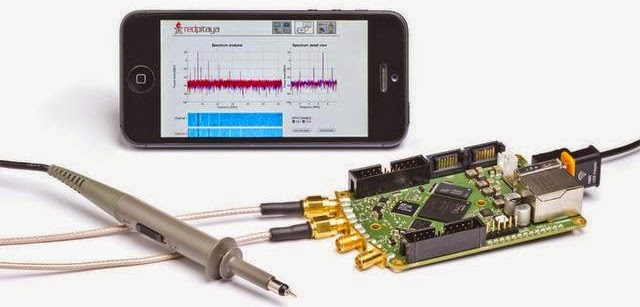
 RED PITAYA – An All-in-One Oscilloscope, Function Generator, Spectrum & Frequency Analyser 


A low cost, portable Control & Instruments device that claims to replace expensive lab and field instruments.

We are in the era of mobiles, gadgets and instruments that are portable, packed with lot of features, have web connectivity and available at a very economical price point. Pick up any electronic gadget or instrument and it will fit in this definition, so why should test and measurement instruments take a back seat!

Introducing RED PITAYA - an innovative single board, low cost, high spec, multifunctional and portable PCB based electronic Test & Measurement Device that aims to replace expensive lab and field instruments.

RED PITAYA – Open Source T&M Device

RED PITAYA – Open Source T&M Device

Features
RED PITAYA is a programmable device powered by Xilinx Zynq7000 SoC that combines dual core ARM & FPGA and runs on Linux. It uses open source ecosystem approach which let users to download standard applications from 'Bazaar' and customize these applications at various programming levels and also develop new applications using source code and documentation available from 'Backyard'.

It is an ideal platform for electronic enthusiasts, students and universities, HAM Radio operators and research institutes.


Red Pitaya In Action


Hardware Specifications of Red Pitaya

Inputs:-
1. The main inputs are two independent channels that run at 125MS/s with 14-bit resolution
2. Four low speed inputs, each at 100kS/s and 12-bit resolution.
Outputs:-
1. Two main analogue outputs at 125MS/s and 14-bit.
2. Four low speed outputs, each at 100kS/s and 12-bit resolution.

Expansion is possible via USB (to add a flash drive, WLAN adapter or camera for instance), and also via a connector that provides 16x FPGA pins for GPIO (e.g. for a custom add-on module). The instrument is typically accessed over Ethernet via a web interface and can be easily connected to local networks. Users can connect to it by simply writing its IP in the address bar for their browsers.

It is also possible to log in, execute remote commands and transfer data via SSH. A handy USB UART interface provides access to the SoC serial console for configuration and debugging.

Hardware Specifications of RED Pitaya


Standard Applications/Functionalities

Oscilloscope - 2 channels @ 125 MS/s 14 bit digital with external or signal based triggering capability
Spectrum Analyser - 2 channels with 50 MHz bandwidth signal with waterfall diagram capability
Arbitrary Waveform Generator - 2 channels @ 125 MHz 14 bit arbitrary waveform generation with external triggering capability

Frequency Response Analyser - 2 channels with 60 MHz bandwidth

The web interface enables access to Red Pitaya’s functionality from the majority of browsers. Applications are available on iPhone, iPad, other smartphones, tablets and PCs.

Software Functionalities, Programming
Red Pitaya can be customised for specific applications above its standard specification. It is based on GNU/Linux operating system and can be customised at different programming levels. Available software interfaces include:
- HDL
- C/C++
- Scripting languages
- Matlab
- HTML based web interfaces

Red Pitaya Target Audience
ELECTRONICS ENTHUSIASTS. Red Pitaya is a great springboard for electronics enthusiasts, because it offers great user interface and can be easily reconfigured for any kind of interaction with outside world by simply modifying the available applications. Out-of-the-box applications, such as oscilloscope or spectrum analyzer, enable fast debugging of electronic projects

STUDENTS. The learning process is simplified by Red Pitaya Backyard containing all the application's source code. Students can start programming by applying incremental changes to the code and publish their work in Bazaar and easily get in touch with a wide range of technologies and knowledge. It is also very appropriate for PhD or other research projects

TEACHERS & PROFESSORS. Red Pitaya is a compact replacement for several expensive instruments and also a universal teaching tool. It enables learning of WEB and embedded application programming, FPGA, signal processing, machine vision applications and it can be controlled by Matlab as well.

HAM RADIO OPERATORS. Amateur radio community uses a wide set of instruments such as SWR meter, network analyzer etc. Red Pitaya has a potential to replace them all. Besides that it can also be used as a radio station or software defined radio (SDR)

RESEARCH INSTITUTIONS. Red Pitaya is very suitable solution for detecting and analyzing fast phenomena, as well as generating or simulating complex signals.

To Conclude
RED Pitaya with its out-of-the-box features, applications & high spec caters to the requirements of all electronics professional working in different areas & on different applications that too at a very affordable price. It is not hard to believe that in coming days RED PITAYA with so much of distinguished features can become inseparable/invaluable device for any electronics lab, design house, R&D center, and university.


Sourced By: EFY:


Sunday, December 7, 2014

0

Simple Stethoscope Circuit Diagram

The stethoscope is a medical or veterinary use tool, in which the professional can hear the heartbeat, breath or other bodily sound of his patient. We can say that the operation of the stethoscope is simple, the recorded sound is amplified and taken directly to the ear by a pipe. The stethoscope is also called phonendoscope, it has two different pickups sound the bell and diaphragm.

The traditional stethoscope is an acoustic equipment, and its pickup of sounds, are specific, the bell and one of the pickups that come in contact with the body, and its function is to capture bass. Have the diaphragm is used to capture the treble, all for a physical process, without the use of electronic circuits.
The Electronic Stethoscope

An electronic stethoscope or estetofone , has the ability to overcome low levels of noise, electronically amplifying body sounds. But this electronic system turns out to be limited the microphone audio frequency responses (pickup) and speaker, something that does not occur in acoustic stethoscopes.

Still there are a large number of companies offering electronic stethoscopes that rely on conversion of acoustic sound waves into electrical signals that can be amplified and processed making a faithful sound system, almost equal to the acoustic. Electronic stethoscopes sold commercially using various systems, the most common is a piezoelectric crystal placed in behind a foam rubber membrane as a pickup.

Simple Stethoscope Circuit Diagram


The evolution of electronic stethoscopes also made possible the emergence of new tests as the phonocardiogram and telemedicine which allowed remote diagnostics.

The circuit simpler and less effective sound detection is achieved by a set of a microphone, an amplifier and a speaker or earphone. This method suffers interference from environmental noise but can be used as a simple electronic stethoscope. Precisely, the simplest is that we show here in this article.

Above the electronic stethoscope circuit, its operation is as follows, one capsule, electret microphone is used as sound pickup, the U1A integrated circuit which is a TL072 has the low noise pre-amplifier function. Your gain is less than 3.9, which is due to the high output impedance of the electret microphone.

The capacitor C2 has a relatively large capacitance, as it filters, leaving only pass the low frequency (20-30 Hz) that are the sounds of a beating heart. The U1B mounted on a Sallen-Key filter low noise with a cutoff frequency of about 103 Hz. R7 and R8 set the gain level of the order of 1.6. The integrated circuit U5 which is a LM386 audio amplifier with an output of 0.25 watts. Part of the U4 integrated circuit can be optional, it is an operational amplifier 741 that controls the two-color LED.

Electronic Stethoscope components list


R1 - 10k ¼ W resistor
R2 - 2.2 ohm ¼ W resistor
R3, R9 - Not used
R4 ¼ W 47 Ohm resistor
R5, R6, R7 - 33K resistor ¼ W
R8 - 56 Ohm resistor ¼ W
R10 - 4k7 ¼ W resistor
R11 - variable resistor of 2.2 logarithmic
R12 - resistor 330 Ohm ¼ W
R13, R15, R16 1K resistor ¼ W
R14 - resistor 3.9 ohm resistor ¼ W
C1, C8 - electrolytic capacitors 470 uF / 16 V
C2 - electrolytic capacitor 4.7 uF / 16 V
C3, C4 - Polyester Capacitors 0.047 uF / 50 V
C5 - ceramic disc capacitor 0.1 uF / 50 V
C6, C7 - electrolytic capacitors 1000 uF / 16 V
U1 TL072
U2, U3 Not used
U4 - 741
U5 - LM386
MIC - electric microphone three terminals

The circuit is very simple and can be mounted on breadboard, on the microphone connection with the circuit should be used shielded cable to prevent noise pickup. You must mount the pickup so that the microphone is placed at a distance from the skin surface but one that is close to the body to protect the microphone from external noise.

Keep the microphone away from the headphones to avoid feedback. Unfortunately, the device offers a very limited application, use it only as a learning circuit, test or demonstration. Link


Tuesday, October 28, 2014

0

Simple Distance Counter Circuit Diagram

Presented here is a simple pedometer circuit. It measures the distance covered by you while walking. It may not work very well for running!

Circuit and working
Fig. 1 shows circuit diagram of the distance counter. The circuit is built around quad 2-input Schmitt trigger CD4093 (IC1), CMOS ripple carry binary counter/divider CD4024 (IC2), decade counter/divider CD4026 (IC3 and IC4), two transistors BC327 (T1, T2) and some other components.

 Fig. 1: Circuit diagram of the distance counter


Fig. 3: An actual-size, single-side PCB for the distance counter


Fig. 4: Component layout for the PCB


Gates N1 and N2 of IC1 form a monostable multivibrator that receives trigger input from tilt or mercury switch S1. When you lift your foot up and touch the ground back during walking, the mercury inside the switch makes a contact with its two metallic leads as shown in Fig. 2. This makes the current to flow between the metallic leads and a pulse is generated at pin 4 of IC1.


   Fig. 2: Open-close operation of

mercury switch
This pulse is fed to pin 1 of IC2 that produces a divide-by-64 counter. Its output is given to inputs of gate N4 of IC1 and the output of N4 is fed to the base of transistor T2 through resistor R8. Transistor T2 drives the decimal point segment of common cathode 7-segment display (DIS1).

IC3 and IC4 are configured as decade counters to drive the 7-segment displays DIS1 and DIS2, respectively. Switch S4 resets these two counters and switch S5 enables DIS1 and DIS2 displays.

Transistor T1 drives the piezobuzzer (PZ1), which beeps after every two steps (one stride), provided switch S2 is closed. DIS1 and DIS2 displays indicate the distance covered in metre (m) and kilometre (km) units, respectively.


Generally, walking step of each individual is slightly different. Here, we assume that a single step is 78cm long, which is the average. According to this, 64 strides equal 100m (that is, 2×0.78×64=99.84m or 100m (approx.)) or 128 steps equal 100m.

DIS1 increments the digit after every 100m distance. That is, DIS1 displays 1 when distance covered is 100m and 2 when distance covered is 200m, and so on. After digit 9 in DIS1, DIS2 increments from 0 to 1 digit. The decimal point (dot) of DIS2 always glows to indicate separation of kilometre from the metre unit.

To save battery power consumption, DIS1 and DIS2 displays illuminate only when you push S5. If you want to reset the counter circuit, both switches S4 and S5 must be pressed simultaneously.


If you want to continuously illuminate DIS1 and DIS2 displays, remove switch S5 and connect the junction of S4 and emitter of transistor T2 to 3V.

Construction and testing
An actual-size, single-side PCB for the distance counter is shown in Fig. 3 and its component layout in Fig. 4.

Mount DIS1 to the right of DIS2 as shown in the PCB so that you get proper readings. For example, if DIS2 shows 5 and DIS1 shows 2, the reading will be 5km and 200m. It means the distance travelled is 5200m.

After assembling the circuit on PCB, enclose it in a suitable plastic case so that you can keep it in your trouser’s pocket or attach it to your belt.

Use 2-pin connector CON1 for 3V battery in the PCB. Also fix switches S2 through S5 on the front side of the case.


Sourced By: EFY : Author :  Yogesh Shukla


Monday, February 10, 2014

0

Electronic Fuse Employs A Relay


hile many power supplies can be set to limit their output current to a defined level, to protect the circuit they are powering, no such protection is available if you are powering a circuit from a battery. If a fault develops, the circuit can blow before you have a chance to disconnect it. Of course, you can fit a fuse in series with the supply line to the circuit under test but it will blow if a fault develops. Or perhaps it won’t blow sufficiently quickly to protect the circuit. And repeatedly having to replace fuses becomes a nuisance as well.

Electronic Fuse Employs A Relay
The alternative is to use an electronic fuse. This circuit uses a relay to make and break the circuit. The current drain of the circuit under test is monitored by a 1O 2W resistor which is placed in series with the supply line. The voltage across this 1O resistor is monitored by op amp IC1a which has an adjustable gain of between 11 and 16, as set by trimpot VR1. The resultant DC voltage from pin 1 of IC1a is fed to pin 5 of IC1b which is configured as a comparator. Trimpot VR2 provides an adjustable voltage reference to pin 6 of IC1b and this is compared with the amplified signal from IC1a.

If IC1b’s threshold is exceeded, its pin 7 goes high and this is fed to Schmitt trigger inverter IC2a which then “sets” the RS flipflop comprising gates IC2c & IC2d. Pin 11 of IC2d then goes high to turn on transistor Q2 and LED1 while pin 4 of IC2b also goes high to turn on Q1 and the relay which then disconnects the load. The circuit stays in this state until the RS flipflop is reset by pushing switch S1. Capacitor Cx, across the feedback resistance of IC1a, is used to simulate a slow-blow or fast-blow fuse and can be selected by trial and error. Changing the gain of IC1a or the value of the sensing resistor changes the fuse rating of the circuit.


Sunday, January 26, 2014

0

Tri-Waveform Generator

The Tri-Waveform Generator can be used for a number of different uses. The one that I use it for is a signal generator to test circuits. The frequency range is 20 to 20khz. and can be adjusted by R1. The duty cycle or the time that the waveform is high and the time that the waveform is low can be adjusted by R4. The purpose of R2 and R3 are to clean up any distortion on the sine wave output. To do this you must hook up the sine wave output to and oscilloscope and adjust R2 & R3 to make the sine wave as accurate as possible.


Social Time

Google Plus
Follow Us
Pinterest
Follow Us

Subscribe to our newsletter

(Get fresh updates in your inbox. Unsubscribe at anytime)