Video of the Day

Showing posts with label Alarm and Security. Show all posts

Friday, November 1, 2019

0

Filter and Polarity Guard for AC/DC Adaptors

The circuit diagram of the filter and polarity guard for the wall AC/DC adaptor is shown in the figure. It is built around a bridge rectifier (BR1), two inductors (L1 and L2), three LEDs, and a few capacitors and resistors.

The circuit has input polarity indicators LED1 and LED2, input fuse F1, input high frequency filter, bridge rectifier BR1, output LC filter and output voltage indicator LED3. Input polarity indicators show the polarities of input AC or DC power connections at connector CON1.

LED1 indicates reverse polarity, whereas LED2 indicates correct polarity of the input signal. Irrespective of input connections, polarities of output voltage at CON2 will not change. LED3 is on when output voltage is present at CON2.

Input filter is built around capacitors C1, C2 and C3 to stop the high frequency noise at input of the device. BR1 is used to ensure that output voltage does not depend on input polarity and, consequently, has fixed polarity. At output of BR1, there is a set of capacitors for reducing ripples and noise coming from the wall adaptor. After that, L1 and L2 further reduce the ripples and noise.

Filter and Polarity Guard for AC/DC Adaptors circuits diagram

Output capacitor C9 provides good filtration at low frequencies and high output peak current. You can calculate the current capacity of this capacitor with the following relationship:

I=C×(dV/dT)

Here, I is the instantaneous current through the capacitor in amperes. C is capacitance in Farads. dV is change in voltage of capacitor in volts. dT is time interval or duration of the pulse applied on the capacitor in seconds. dV/dT is the instantaneous rate of voltage change over the capacitor as volts/second.

L1 and L2 are selected according to required output current and suppression of noise and ripples. All capacitors should be rated for at least 35V because most are designed for 19V and above.
Construction and testing

It is easy to assemble the circuit on a Veroboard. The circuit does not require any adjustments to work properly. Input fuse F1 is selected according to the wall adaptor output rating.

Using the circuit is simple. Connect output of the adaptor to CON1. Then, connect output voltage from CON2 to the load or target device.


The circuit is simple but useful for wall AC/DC adaptors where it is important to reduce ripples and noise, and improve transient response of the adaptors. It can also be used in a wide range of switching and analogue power supplies.

The circuit has been developed for 26V and 19V wall adaptors, but by replacing some components, it can be used for other wall adaptors with output voltage starting from 5V. When input polarity is fixed, the bridge can be replaced with simple diodes depending on requirement.

Sourced By : EFY Author : Petre Tzv Petrov


Wednesday, August 1, 2018

0

A Doorbell for the Deaf

This circuit provides a delayed visual indication when a door bell switch is pressed. In addition, a DPDT switch can be moved from within the house which will light a lamp in the door bell switch. The lamp can illuminate the words "Please Wait" for anyone with walking difficulties. 


A Doorbell for the Deaf Circuit Diagram :

A Doorbell for the Deaf Circuit Diagram


Notes :
The circuit uses standard 2 wire doorbell cable or loudspeaker wire. In parallel with the doorbell switch, S1, is a 1N4001 diode and a 12 volt 60mA bulb. The bulb is optional, it may be useful for anyone who is slow to answer the door, all you need to do is flick a switch inside the house, and the bulb will illuminate a label saying Please Wait inside the doorbell switch or close to it. The double pole double throw switch sends the doorbell supply to the lamp, the 22 ohm resistor is there to reduce current flow, should the doorbell switch, S1 be pressed while the lamp is on. The resistor needs to be rated 10 watts, the 0.5 Amp fuse protects against short circuits.

When S2 is in the up position (shown as brown contacts), this will illuminate the remote doorbell lamp. When down, (blue contacts) this is the normal position and will illuminate the lamp inside the house. Switch S1 will then charge the 47u capacitor and operate the transistor which lights the lamp. As a door bell switch is only pressed momentarily, then the charge on the capacitor decays slowly, resulting in the lamp being left on for several seconds. If a longer period is needed then the capacitor may be increased in value.


Saturday, October 24, 2015

0

Simple Laser Based Security Lock Circuit Diagram

Presented here is a security system that uses an inexpensive laser torch which is usually available with a key ring. The advantage of this security lock is that you can use any laser torch or pointer that is easily available in toy shops. It employs minimal input keys and yet is very secure. It can be used as a door lock, briefcase lock or any other application related to an electronic locking system.

Circuit and working
The block diagram of a laser-based security lock is shown in Fig. 1 and its schematic diagram in Fig. 2. Switches S1 and S2 work as security input keys and switch S3 is used for opening the lock manually. The lock can be an electric strike installed on the door frame to allow access with an access control system or any electronic remote control system.


Fig. 1: Block diagram of the laser based security lock

Electric strikes are generally available in two configurations—fail-secure and fail-safe. In fail-secure configuration, applying electric current to the strike causes it to open; whereas in fail-safe configuration, applying electric current to the strike causes it to lock. A fail-secure configuration is used in this project.

Opening the lock. The use of switch S2, pressing and releasing of switch S1 and supplying the laser pulses at the right time are the security features of this circuit. Switch S2 should not be released during the entire operation, otherwise the counter will get reset and you will not be able to open on the lock.

Circuit diagram of the laser based security lock
Fig. 2: Circuit diagram of the laser based security lock


When switch S1 is pressed, the first in-built timer of IC2 is triggered. Its output pin 5 goes high for four seconds. LED1 glows and transistor T3 conducts. During this time, the collector of T3 becomes low, which in turn pulls the clock enable pin (pin 13) of IC1 to low state. This enables the counter (IC1) to count. During this time, five laser pulses are applied (by you) at photo sensor T1. These signal pulses go to clock pin 14. LED4 glows and T2 conducts at the fifth pulse. This triggers the in-built second timer of IC2. Its output pin 9 goes high for two seconds. The high state is indicated by the glowing of LED2. When LED2 goes off, you press switch S1 and release it. The first timer is triggered again and its output is high for four seconds. During this time, you send another five pulses of laser beam towards the sensor. At the fifth pulse, LED3 glows and transistor T4 conducts. This action triggers IC3 and its output pin 3 goes high for ten seconds. That is, the lock opens for ten seconds.
 The lock driver circuit is connected to output pin 3 of IC3. The circuit is powered off a 5V DC supply. Normally the electric lock or electric strike works off a 12V DC. To make the circuit simple, the lock driver section is not shown here.

Construction and testing
An actual-size, single-side PCB layout of the laser-based security lock is shown in Fig. 3 and its component layout in Fig. 4.

Mount the components on the PCB to avoid any assembly errors. Enclose the circuit in a suitable box. Mount switches S1, S2 and S3 at appropriate locations. If the circuit is to be used as a door lock, photo sensor T1, switches S1 and S2 should be mounted outside the door frame. The photo sensor should be enclosed in the box with a suitable contraption so that it can receive the laser beam properly. Switch S3 should be installed on other side of the wall near the door frame.

 An actual-size PCB layout for the laser based security lock circuit
 An actual-size PCB layout for the laser based security lock circuit  


 Component layout of the PCB 

While pressing switches S1 and S2 simultaneously, point the laser torch toward the photo transistor sensor T1 and press on/off button of the laser torch five times within four seconds. Release switch S1 while pressing switch S2. Wait for two seconds till LED2 goes off. Keeping S2 pressed, press S1 and release it, press on/off button of laser torch five times again. The lock will open for ten seconds and then close automatically. The lock can also be opened from the inside (for ten seconds) by pressing switch S3.

Sourced by : EFY


Sunday, August 16, 2015

0

Sequential Tilt-Motion Lock

Here is a project for locking and unlocking with a tilt sensor by tilting it in a defined sequence. It uses an accelerometer module to detect the tilt motion. If the sequence matches with the predefined motion sequence, the lock opens. You can build this lock for a briefcase, ballot box, portable cashbox or even as a door-lock using suitable mechanical arrangement.

Circuit and working
Fig. 1 shows circuit diagram of the sequential tilt-motion lock. The circuit is built around Arduino Uno board (Board1), accelerometer module (ACC.1), solenoid lock/electric strike and a few other components.

Circuit diagram of sequential tilt-motion lock
Fig. 1: Circuit diagram of sequential tilt-motion lock

Arduino Uno board. Arduino is an open source electronics prototyping platform based on flexible, easy-to-use hardware and software. It is intended for artists, designers, hobbyists and anyone interested in creating interactive objects or environments.
Arduino Uno is a board based on ATmega328 microcontroller. It consists of 14 digital input/output pins, six analogue inputs, a USB connection for programming the on-board microcontroller, power jack, an ICSP header and a reset button. It is operated with a 16MHz crystal oscillator and contains everything needed to support the microcontroller. It is very easy to use as the user simply needs to connect it to a computer with a USB cable, or power it with an AC-to-DC adaptor or battery to get started. The microcontroller on the board is programmed using Arduino programming language and Arduino development environment.

Pins A0, A1, A2, A3, A4 and A5 of Board1 are connected to pins ST, Z-axis, Y-axis, X-axis, GND and Vcc of the accelerometer module, respectively. Pin 10 of Board1 is connected to solenoid driver transistor through which the solenoid lock is connected.

Accelerometer module. An accelerometer is an electromechanical device that measures acceleration. The accelerometer module used here is based on ADXL335 triple-axis accelerometer from Analog Devices. The sensor has a full sensing range of ±3g.

The microcontroller in Board1 receives data at pins A1, A2 and A3 for z, y and x axes, respectively, from the accelerometer. This data is continuously compared by Board1 with predefined values for each axis. If the received sequence matches, Board1 unlocks the lock, which is either a solenoid lock or any other suitable magnetic lock. (We used a 12V electric strike for testing.) Glowing of LED1 indicates that the lock is open.

Software
The software for this project is written in Arduino programming language. The Arduino Uno is programmed using Arduino IDE software. ATmega328 on Arduino Uno comes with a boot loader that allows you to upload new code to it without the use of external hardware programmer. It communicates using the STK500 protocol. You can also bypass the boot loader and program the microcontroller through in-circuit serial programming (ICSP) header, but boot loader programming is quicker and easier. Select the correct board from ‘Tools → Board’ in Arduino IDE and burn the program (sketch) through standard USB port in the computer.

Fig. 2: An actual-size PCB layout for the sequential tilt-motion lock

Fig. 3: Component layout for the PCB


Construction and testing

An actual-size (Arduino shield type), single-side PCB for the sequential tilt-motion lock is shown in Fig. 2 and its component layout in Fig. 3. Assemble the circuit on the recommended PCB to minimize assembly errors.

To test the circuit for proper functioning, switch on S1 and verify correct 12V supply for the circuit at TP1 with respect to TP0.

The neutral position of accelerometer module is parallel to the earth’s surface. The +Y and +X axes are marked on the accelerometer module. The default tilt sequence of this circuit defined in the source code is -X, -Y, -X, +Y, -Y. If the tilt sequence is correct, you can observe the glowing of an in-built LED (not shown here) connected to pin 13 of Arduino board. If you want to change the sequence, change it in the source code, recompile the program and burn into the microcontroller.

To open the lock, switch on S1 and tilt the circuit sequentially, as mentioned above, within one minute. If correct action is not completed within one minute, you need to repeat the tilt sequence from the start to unlock it. To close the lock, just switch off the circuit using on/off switch S1.


Soueced By : EFY Author:  Akhil Kaushik


Monday, July 13, 2015

0

Versatile Audio-Visual Alarm Circuit Diagram

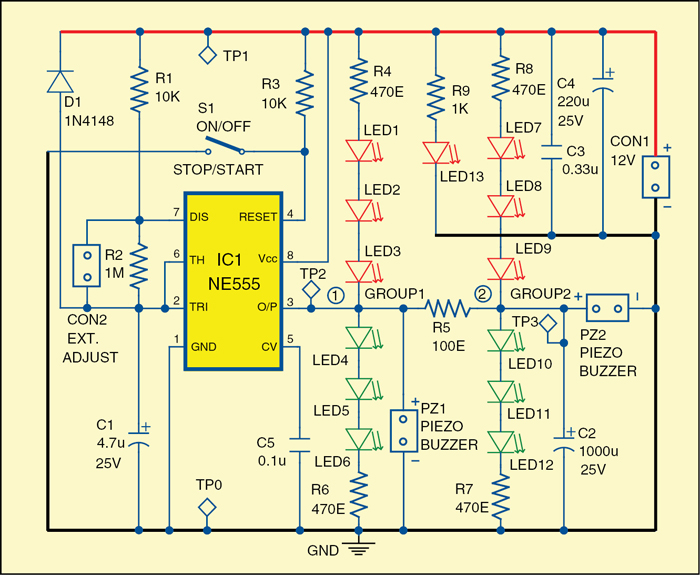
This circuit uses an NE555 timer IC, some LEDs, a couple of piezo buzzers and a few other components to produce audio-visual effects as per your requirement. The timer NE555 and its equivalents are widely used for all sorts of audio and visual indications, such as door alarms. But the sound produced by these circuits may not be always pleasant to hear, or the light produced may not be visually appealing. With this circuit you can get different audio-visual effects.

Here we use LEDs for visual indication and buzzers for audible alarms as they require relatively low current to operate. By simply connecting some resistors and capacitors to NE555 we can obtain some interesting visual and audible effects as described here.

Circuit and working
Fig. 1 shows the circuit of the versatile audio-visual alarm which is built around timer NE555 (IC1), LEDs, buzzers and some resistors and capacitors. Resistors R1 and R2 and capacitor C1 determine the frequency of the LEDs’ blinking. The frequency is selected usually within the range of 0.1Hz to 20Hz, depending on your requirement. Values of resistors R1 and R2 can be above 1-kilo-ohm. Capacitor C1’s value can be between 1µF and 1000µF.


Versatile Audio-Visual Alarm Circuit Diagram
Fig. 1: The versatile audio-visual alarm circuit


Fig. 2: Actual-size, single-side PCB for the circuit
  
Fig. 3: Component layout for the PCB


Timer NE555 drives two outputs, namely, Group1 and Group2. Group1 is built around resistors R4 and R6 along with LED1 through LED6. Group2 is built around resistors R7 and R8 along with LED7 through LED12.


Each of the groups can be configured to get different outputs. For example, in Group1 you can use only the LEDs (LED1 through LED3) connected to +12V, or only the LEDs (LED4 through LED6) connected to the ground, or both branches of these LEDs, or only piezo buzzer PZ1, or PZ1 with any combination of the LEDs, or you can omit the entire Group1.

The components in Group2 can form the same combinations as the components in Group1. The difference between the Group1 and Group2 is the use of resistor R5 and capacitor C2. These two components give light-decay effect to the LEDs and a pleasant low-pitch sound to piezo buzzer in Group2. Value of resistor R5 can be between 75-ohm and 1-kilo-ohm and that of capacitor C2 between 47µF and 1000µF.

At point 1 (TP2) in the circuit you can see a rectangular wave signal. At point 2 you can see a triangular or trapezoidal-like signal. The signals at points 1 and 2 should go low, almost to zero, and should go high, almost to 12V supply voltage.

Power supply used is 12V, but it can be in the range of 4.5V to 15V as well, depending on the number of LEDs used in each branch. Higher number of LEDs will require higher voltage. LED13 glows when power supply is connected in the circuit.

Resistors R4, R6, R7 and R8 are selected according to the number and type of the LEDs used. If the values of these resistors are too low, the output of the timer will be overloaded and the LEDs in the upper and the lower branches will get activated simultaneously.
 
Overloading may also damage the NE555 timer. It is suggested to keep the total output current drawn from NE555 below 100mA.

On/off switch S1 is used to start or stop the alarm. Connector CON2 is an optional input point for connecting a variable element, such as a preset, for adjusting or varying the frequency of the square signal for more audio-visual effects.

Construction and testing
An actual-size, single-side PCB for the versatile audio-visual alarm is shown in Fig. 2 and its component layout in Fig. 3. After assembling the circuit on PCB, enclose it in a suitable plastic box.

Connect piezo buzzers PZ1 and PZ2 at their provided places in the PCB. Also connect 2-pin terminal CON1 for power supply. Connect CON2 for external input (optional). Before using the alarm circuit, check at the test points given in the table.


Sourced By: EFY Author:  Petre Tzv Petrov


Monday, June 29, 2015

0

Simple Versatile Audio-Visual Alarm Circuit Diagram

This circuit uses an NE555 timer IC, some LEDs, a couple of piezo buzzers and a few other components to produce audio-visual effects as per your requirement. The timer NE555 and its equivalents are widely used for all sorts of audio and visual indications, such as door alarms. But the sound produced by these circuits may not be always pleasant to hear, or the light produced may not be visually appealing. With this circuit you can get different audio-visual effects.

Here we use LEDs for visual indication and buzzers for audible alarms as they require relatively low current to operate. By simply connecting some resistors and capacitors to NE555 we can obtain some interesting visual and audible effects as described here.

Circuit and working
Fig. 1 shows the circuit of the versatile audio-visual alarm which is built around timer NE555 (IC1), LEDs, buzzers and some resistors and capacitors. Resistors R1 and R2 and capacitor C1 determine the frequency of the LEDs’ blinking. The frequency is selected usually within the range of 0.1Hz to 20Hz, depending on your requirement. Values of resistors R1 and R2 can be above 1-kilo-ohm. Capacitor C1’s value can be between 1µF and 1000µF.

Simple Versatile Audio-Visual Alarm Circuit Diagram


Simple Versatile Audio-Visual Alarm Circuit Diagram

Fig. 1: The versatile audio-visual alarm circuit


Fig. 2: Actual-size, single-side PCB for the circuit
  
 Fig. 3: Component layout for the PCB

Timer NE555 drives two outputs, namely, Group1 and Group2. Group1 is built around resistors R4 and R6 along with LED1 through LED6. Group2 is built around resistors R7 and R8 along with LED7 through LED12.


Each of the groups can be configured to get different outputs. For example, in Group1 you can use only the LEDs (LED1 through LED3) connected to +12V, or only the LEDs (LED4 through LED6) connected to the ground, or both branches of these LEDs, or only piezo buzzer PZ1, or PZ1 with any combination of the LEDs, or you can omit the entire Group1.

The components in Group2 can form the same combinations as the components in Group1. The difference between the Group1 and Group2 is the use of resistor R5 and capacitor C2. These two components give light-decay effect to the LEDs and a pleasant low-pitch sound to piezo buzzer in Group2. Value of resistor R5 can be between 75-ohm and 1-kilo-ohm and that of capacitor C2 between 47µF and 1000µF.

At point 1 (TP2) in the circuit you can see a rectangular wave signal. At point 2 you can see a triangular or trapezoidal-like signal. The signals at points 1 and 2 should go low, almost to zero, and should go high, almost to 12V supply voltage.

Power supply used is 12V, but it can be in the range of 4.5V to 15V as well, depending on the number of LEDs used in each branch. Higher number of LEDs will require higher voltage. LED13 glows when power supply is connected in the circuit.

Resistors R4, R6, R7 and R8 are selected according to the number and type of the LEDs used. If the values of these resistors are too low, the output of the timer will be overloaded and the LEDs in the upper and the lower branches will get activated simultaneously.

Overloading may also damage the NE555 timer. It is suggested to keep the total output current drawn from NE555 below 100mA.

On/off switch S1 is used to start or stop the alarm. Connector CON2 is an optional input point for connecting a variable element, such as a preset, for adjusting or varying the frequency of the square signal for more audio-visual effects.

Construction and testing
An actual-size, single-side PCB for the versatile audio-visual alarm is shown in Fig. 2 and its component layout in Fig. 3. After assembling the circuit on PCB, enclose it in a suitable plastic box.

Connect piezo buzzers PZ1 and PZ2 at their provided places in the PCB. Also connect 2-pin terminal CON1 for power supply. Connect CON2 for external input (optional). Before using the alarm circuit, check at the test points given in the table.


Sourced By: EFY Author :  Petre Tzv Petrov


Friday, June 5, 2015

0

Simple Motor Bike Brake Horn Circuit Diagram

The circuit can be operated from 4.5V to 12V DC or direct from the brake point of the motor-bike, Resistor R7 should be replaced with 1-ohm. 1/2W in case of an 8-ohm speaker. T5 is a driver transistor. C3 polarity can be reversed for a sudden off of the circuit.

Simple Motor Bike Brake Horn Circuit Diagram


Simple Motor Bike Brake Horn Circuit Diagram


PARTS LIST
Resistors (all ¼-watt, ~+mn~ 5% Carbon)
R1, R7 = 2.2 KΩ
R2, R4 = 820 Ω
R3, R5 = 470 Ω
R6 = 4.7 KΩ
R8 = 10 KΩ
R9 = 4.7 Ω, 0.5W

Capacitors
C1 = 22 µF/25v
C2 = 4.7 µF/63V
C3 = 100v/16V
C4 = 0.047 µF
C5 = 0.01 µF

Semiconductors
T1 – T4 = BC148B
T5 = SL100
Miscellaneous
LS1 = 4Ω speaker


Thursday, April 16, 2015

0

Simple Sensitive LPG Leakage Alarm Circuit Diagram

Here is an ultra-sensitive LPG sensor that generates loud beeps when it senses any gas leakage. It detects vapours of liquefied petroleum gas anywhere between 200 and 10,000 ppm and drives a piezobuzzer to catch attention for immediate action. The buzzer beeps until the concentration of gas in the air decreases to a safe level. The circuit uses an MQ6 gas sensor, which is designed to sense LPG, propane and isobutane gases.

Circuit and working
Fig. 1 shows the circuit of the LPG sensor. The circuit is built around 5V voltage regulator 7805 (IC1), gas sensor MQ6 (GS1), counter IC 4060 (IC2) and a few discrete components.


GS1 is a six-pin gas sensor that can detect very small traces of LPG in the air and has a swift response time. However, it has very less sensitivity to alcohol and smoke. The sensor’s output is in the form of resistance.

Component layout for the PCB

Fig. 1: Circuit of the sensitive LPG sensor

As indicated in Fig. 1, the pins of GSI are H, A and B, two each on either side. H pins are for the heater with no polarity. Input pins A or B and output pins A or B can be connected either way round.

The coil heater inside the sensor can be easily heated with 5V DC. If pin A is connected to 5V DC through variable resistor VR1, use pin B as the output or vice versa. Both A and B pins can be shorted. In short, H pins are connected to positive and negative rails, A or B pin to 5V DC, and B or A for output.

The resistance value of GSI is different for various kinds and concentration of gases. So when using this sensor, sensitivity arrangement is very important. For accurate detection, it is necessary to calibrate the sensor for 1000 ppm of LPG concentration in the air with load resistance of about 20 kilo-ohms. (In the datasheet, the load resistance range of MQ6 is mentioned as 10 kilo-ohms to 47 kilo-ohms.)


Fig. 2: An actual-size, single-side PCB for sensitive LPG sensor

Fig. 3: Component layout for the PCB

Preset VR1 is used to adjust the sensitivity of the sensor to a particular gas concentration. Output from the sensor is connected to the base of transistor T1, which acts as a switch to trigger the alarm generator built around IC2.

IC2 is a binary counter IC that oscillates using capacitor C2 and resistor R5. Transistor T1 controls the reset pin (pin 12) of IC2. When the reset pin is high IC2 does not oscillate, and when this pin goes low IC2 starts oscillating.

Working of the circuit is simple. When the sensor detects LPG in the air, its output becomes high and transistor T1 conducts to make reset pin of IC2 low. This triggers IC2 to oscillate, which is indicated by LED1. After a few seconds, the buzzer starts beeping to indicate gas leakage.

The circuit works off 12V DC from a battery (BATT.1) or you can use an adaptor. IC1 provides regulated 5V DC supply for the sensor and IC2.

 Construction and testing
An actual-size, single-side PCB for sensitive LPG sensor is shown in Fig. 2 and its component layout in Fig. 3. After assembling the circuit on a PCB, enclose it in a suitable case with an opening to allow the gas to enter. Place the unit near the LPG cylinder or gas stove within a distance of one metre. Vary preset VR1 to adjust the sensitivity of the sensor.

To test the circuit, check 12V at test point TP1 with respect to TP0 to verify the correct power supply. Place the unit near the gas stove burner and turn on the burner for a few seconds without igniting. Then, turn ’the burner ‘off’ and adjust VR1 until you see LED1 glowing. TP3 should be low at this moment.


Sourced By: EFY : Author Name :  D. Mohan Kumar


Thursday, February 26, 2015

0

Diplomatic Optical Burglar Alarm Circuit Diagram

This is the simple Diplomatic Optical Burglar Alarm Circuit Diagram. This optical burglar alarm uses two 555 timer ICs (IC1 and IC2). Both the ICs are wired as astable multivibrators. The first astable multivibrator built around IC1 produces low frequencies, while the second astable multivibrator built around IC2 produces audio frequencies. General-purpose Darlington photo-transistor T1 is used as the light sensor. To increase the sensitivity of the circuit, NPN transistor T2 is used.

Place phototransistor T1 where light falls on it continuously. Phototransistor T1 receives light to provide base voltage to transistor T2. As a result, transistor T2 conduct to keep reset pin 4 of IC1 at low level. This disables the first multivibrator (IC1) and hence the second multivibrator (IC2) also remains reset so the alarm (LS1) does not sound.


Diplomatic Optical Burglar Alarm Circuit Diagram


Diplomatic Optical Burglar Alarm Circuit Diagram


When light falling on Darlington phototransistor T1 is obstructed, transistor T2 stops conducting and reset pin 4 of IC1 goes high. This enables the first multivibrator (IC1) and hence also the second multivibrator (IC2). As a result, a beep tone is heard from speaker LS1. The beep rate can be varied by using preset VR1, while the output frequency of IC2 can be varied by using another preset VR2. This circuit works off a simple 6V-12V DC power supply.


PARTS LIST
Resistors (all ¼-watt, ± 5% Carbon unless stated otherwise)
R1, R5 = 1 KΩ
R2 = 100 KΩ
R3 = 4.7 KΩ
R4 = 10 KΩ
VR1 = 1 MΩ
VR2 = 100 KΩ
Capacitors
C1 = 1 µF/16V
C2 = 0.01 µF
C3 = 0.047 µF
C4 = 0.01 µF
C5 = 47 µF/25V
Semiconductors
IC1, IC2 = NE555
T1 = 2N5777 Photo Transistor
T2 = BC547
LED1 = RED LED
Miscellaneous
LS1 = 8Ω / 0.5W


Sunday, January 11, 2015

0

Versatile Audio-Visual Alarm Circuit Diagram

This circuit uses an NE555 timer IC, some LEDs, a couple of piezo buzzers and a few other components to produce audio-visual effects as per your requirement. The timer NE555 and its equivalents are widely used for all sorts of audio and visual indications, such as door alarms. But the sound produced by these circuits may not be always pleasant to hear, or the light produced may not be visually appealing. With this circuit you can get different audio-visual effects.

Here we use LEDs for visual indication and buzzers for audible alarms as they require relatively low current to operate. By simply connecting some resistors and capacitors to NE555 we can obtain some interesting visual and audible effects as described here.

Circuit and working
Fig. 1 shows the circuit of the versatile audio-visual alarm which is built around timer NE555 (IC1), LEDs, buzzers and some resistors and capacitors. Resistors R1 and R2 and capacitor C1 determine the frequency of the LEDs’ blinking. The frequency is selected usually within the range of 0.1Hz to 20Hz, depending on your requirement. Values of resistors R1 and R2 can be above 1-kilo-ohm. Capacitor C1’s value can be between 1µF and 1000µF.

Versatile Audio-Visual Alarm Circuit Diagram

Fig. 1: The versatile audio-visual alarm circuit


Fig. 2: Actual-size, single-side PCB for the circuit

 Fig. 3: Component layout for the PCB


Timer NE555 drives two outputs, namely, Group1 and Group2. Group1 is built around resistors R4 and R6 along with LED1 through LED6. Group2 is built around resistors R7 and R8 along with LED7 through LED12.


Each of the groups can be configured to get different outputs. For example, in Group1 you can use only the LEDs (LED1 through LED3) connected to +12V, or only the LEDs (LED4 through LED6) connected to the ground, or both branches of these LEDs, or only piezo buzzer PZ1, or PZ1 with any combination of the LEDs, or you can omit the entire Group1.

The components in Group2 can form the same combinations as the components in Group1. The difference between the Group1 and Group2 is the use of resistor R5 and capacitor C2. These two components give light-decay effect to the LEDs and a pleasant low-pitch sound to piezo buzzer in Group2. Value of resistor R5 can be between 75-ohm and 1-kilo-ohm and that of capacitor C2 between 47µF and 1000µF.

At point 1 (TP2) in the circuit you can see a rectangular wave signal. At point 2 you can see a triangular or trapezoidal-like signal. The signals at points 1 and 2 should go low, almost to zero, and should go high, almost to 12V supply voltage.

Power supply used is 12V, but it can be in the range of 4.5V to 15V as well, depending on the number of LEDs used in each branch. Higher number of LEDs will require higher voltage. LED13 glows when power supply is connected in the circuit.

Resistors R4, R6, R7 and R8 are selected according to the number and type of the LEDs used. If the values of these resistors are too low, the output of the timer will be overloaded and the LEDs in the upper and the lower branches will get activated simultaneously.


Overloading may also damage the NE555 timer. It is suggested to keep the total output current drawn from NE555 below 100mA.

On/off switch S1 is used to start or stop the alarm. Connector CON2 is an optional input point for connecting a variable element, such as a preset, for adjusting or varying the frequency of the square signal for more audio-visual effects.

Construction and testing
An actual-size, single-side PCB for the versatile audio-visual alarm is shown in Fig. 2 and its component layout in Fig. 3. After assembling the circuit on PCB, enclose it in a suitable plastic box.

Connect piezo buzzers PZ1 and PZ2 at their provided places in the PCB. Also connect 2-pin terminal CON1 for power supply. Connect CON2 for external input (optional). Before using the alarm circuit, check at the test points given in the table.


Tuesday, December 30, 2014

0

Door-Knock or Vibration Alarm Circuit Diagram

This is a simple circuit that activates an alarm when there is a knock on the door or there are any vibrations due to movement of heavy goods or furniture. The circuit uses readily available components.

Circuit and working
The circuit is built around quad-opamp LM324 (IC1), which is configured in amplifier mode. It uses the piezoelectric element of a piezo buzzer as the input sensor, two transistors BC547 (T1 through T2), a piezo buzzer and some other components for the alarm circuit. Fig. 1 shows the circuit diagram of the door-knock alarm.

The reference voltage at pin 3 of IC1 is set by trimming potmeter VR1. The piezoelectric element plate is fixed at the centre of the door using cello tape. Apply a small quantity of adhesive on the edges between the plates. Wires from the piezo element are connected at CON2. These generate an input pulse when vibrations are caused by knocking on the door. The pulse is amplified by op-amp A1 of IC1. Remaining three op-amps of quad IC LM324 are not used here.

The output of A1 of LM324 from pin 1 is further amplified by transistors T1 and T2 to drive the piezo buzzer or relay. Because of the presence of high-value capacitor C5, the buzzer remains active for a few seconds. The circuit is powered by 9V/12V power supply. Sensitivity of the circuit can be adjusted by 1M potmeter VR1.


Door-Knock or Vibration Alarm Circuit Diagram
Fig. 1: Circuit diagram of a door-knock alarm

In place of piezo buzzer PZ1, you can use 9V/12V single-changeover relay connected to an amplifier for louder sounds.

Construction and testing
An actual-size, single-side PCB for the alarm is shown in Fig. 2 and its component layout in Fig. 3. After assembling the circuit on the PCB, enclose it in a suitable plastic box.


An actual-size PCB layout of the circuit
Fig. 2: An actual-size PCB layout of the circuit
   
Component layout of the PCB
 Fig. 3: Component layout of the PCB


Before using the circuit, ensure that supply voltage is correct.


Sourced By: EFY Author :  Pradeep G


Wednesday, December 10, 2014

0

Simple Two 555 Timers Bell Circuit Diagram

This is the Simple Two 555 Timers Bell Circuit Diagram. This simple scheme uses two Bell 555 timer. The frequency controlled capacitors, which should be preserved are almost identical in value with each other to achieve the best results. Fine tuning is done with the R1 and R2. The decay time is controlled by R3.
 

Simple Two 555 Timers Bell Circuit Diagram

 
Simple Two 555 Timers Bell Circuit Diagram


Saturday, December 6, 2014

0

Monitor and Protection Alarm Over Current Circuit Diagram

The electronic circuit described in this article's main function remote monitoring of power consumption (over current) in a domestic mains alternating current. This monitoring is necessary in many systems, especially in electronic counters, power supplies, AC, inverters, converters, etc.

The operation of the circuit is simple, to be connected to the power grid, and when the circuit detects a consumption in the electric network of more than 5 mA he lights LA1 signal lamp. The device can work with currents of several amperes, it depends on the diode used in D1 and D2. The Ti1 transistor is turned on when the D1 and D2 drop exceeds a certain level.


Monitor and Protection Alarm Over Current Circuit Diagram


Fuse F1 must of course be dimensioned to suit the application and current limit circuit. When Ti1 leads the alternating current can flow through the capacitor, and the triac is triggered, so that lights the lamp LA1.


The above circuit is a current alarm of some changes, there is a bridge rectifier formed by diodes D4 to D7, which was added only to supply the voltage to the coil of the relay Re1, that when the current through D2 exceeds a di-certain set level. The capacitor C1, may need to be resized to fit the sensitivity of the chosen relay coil.

Conclusion

Ti1 can be any transistor, just make sure that it can work with voltages up to 700 V. For D1 and D2, are recommended diodes 1N4000 series that can be used for currents up to 1 Amp or types 1N5400 supporting up 3 Amps. Watch out! This circuit works with the current network continues to play home that can be fatal, read our text on the Site Responsibility.


Friday, November 21, 2014

0

IC 555 Burglar Alarm Circuit Diagram

Burglar alarm circuit or Theft alarm circuits are available in several forms. The above circuit was one of that kind using timer IC 555 as the main component. The circuit is very easy to construct and the cost of this circuit is also very less. So we can implement this circuit by our own and install this circuit in our home so that you can improve your knowledge and it also adds protection to your home.

Using IC 555 Burglar Alarm Circuit Diagram

Using IC 555 Burglar Alarm Circuit Diagram


The working of this circuit is very easy to understand.In the above circuit IC 555 was used as a Astable multivibrator.The Astable multivibrator puts out a continuous stream of rectangular pulses having a specified frequency. Thus by using the Astable multivibrator we can produce continuous frequency which was given as input to the speaker which makes an alarm sound in case of any disturbance in its trip wire. Pin diagram of IC 555 was given below for your better understanding.


Now we can see how we can change the Astable Multivibrator to a alarm circuit.In the above circuit the 4th pin (RESET pin) was connected to the ground using the thin strand of copper wire which is used as a trip in this circuit.The function of the 4th pin that it resets the timing interval when it was connected to the ground.

When the wire was connected the Multivibrator cant produce the rectangular pulses of constant frequency.When the copper strand is cut off then the 4th pin will have no connection with the ground.Therefore IC 555 produces the output pulse and which was given as input to the speaker thus it drives the speaker to give a noise which would scare the burglar away.Thus your homemade effective burglar circuit is ready Sourced by: Circuitsproject


Wednesday, November 19, 2014

0

Simple Miniature Loop Alarm Circuit Diagram

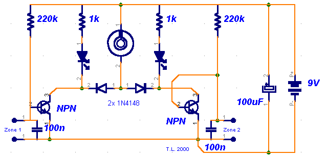
This is the Simple Miniature Loop Alarm Circuit Diagram. The simple construction, reliable operation, very small power consumption, and, most of all, small size. I started with CMOS logic gates, but was soon forced to abandon the concept after a few unsuccessful (and far too complicated) attempts. Then I suddenly realized that a simple transistor switch might do the job and I was right.


Simple Miniature Loop Alarm Circuit Diagram


Simple Miniature Loop Alarm Circuit Diagram


Notes

As you can clearly see from the schematics, the circuit is utterly primitive and consists of two identical transistor switches. Each has its own alarm LED and they're coupled to a neat 82dB buzzer. The two 1N4148 diodes are used to prevent a signal from one sensor from triggering both LEDs. The sensors used are either wire loops or normally closed reed switches or even a combination of both. You could, for example, tie a wire loop to your suitcase and place a reed switch to the door of your hotel room.Since this little alarm is intended to be kept in arms reach at all times, there aren't any provisions for automatic shutdown after a certain period of time. 

The buzzer will sound until you turn the whole circuit off or connect the wire loop back to the jumpers. The same goes for the two LEDs, each indicating its own zone.Construction is not critical and there aren't any traps for the novice. The two 100n capacitors aren't really necessary, I just included them to make sure that there is no noise interference coming from the long wire loops. For transistors, you can use any NPN general-purpose audio amplifiers/switches (BC 107/108/109, BC 237/238, 2N2222, 2N3904...). Assemble the circuit on perf board. Together with the buzzer and a 9V battery, it should easily fit in a pocket-sized plastic box smaller than a pack of cigarettes. A fresh battery should suffice for weeks of continuous operation. 


Author: Tomaz Lazar - Ljubljana, Slovenia


Monday, November 17, 2014

0

Using IC 555 Burglar Alarm Circuit Diagram

Burglar alarm circuit or Theft alarm circuits are available in several forms. The above circuit was one of that kind using timer IC 555 as the main component. The circuit is very easy to construct and the cost of this circuit is also very less. So we can implement this circuit by our own and install this circuit in our home so that you can improve your knowledge and it also adds protection to your home.

Using IC 555 Burglar Alarm Circuit Diagram

Using IC 555 Burglar Alarm Circuit Diagram


The working of this circuit is very easy to understand.In the above circuit IC 555 was used as a Astable multivibrator.The Astable multivibrator puts out a continuous stream of rectangular pulses having a specified frequency. Thus by using the Astable multivibrator we can produce continuous frequency which was given as input to the speaker which makes an alarm sound in case of any disturbance in its trip wire. Pin diagram of IC 555 was given below for your better understanding.


Now we can see how we can change the Astable Multivibrator to a alarm circuit.In the above circuit the 4th pin (RESET pin) was connected to the ground using the thin strand of copper wire which is used as a trip in this circuit.The function of the 4th pin that it resets the timing interval when it was connected to the ground.

When the wire was connected the Multivibrator cant produce the rectangular pulses of constant frequency.When the copper strand is cut off then the 4th pin will have no connection with the ground.Therefore IC 555 produces the output pulse and which was given as input to the speaker thus it drives the speaker to give a noise which would scare the burglar away.Thus your homemade effective burglar circuit is readySourced by: Circuitsproject


0

Cheap and Simple Gate Alarm Circuit Diagram

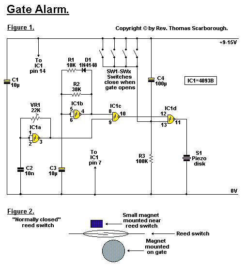
This is the Cheap and Simple Gate Alarm Circuit Diagram. A cheap and simple gate alarm made from a single CMOS Integrated Circuit. 

 Cheap and Simple Gate Alarm Circuit Diagram

Cheap and Simple Gate Alarm Circuit Diagram


Circuit Notes
Figure 1 represents a cheap and simple Gate Alarm, that is intended to run off a small universal AC-DC power supply.

IC1a is a fast oscillator, and IC1b a slow oscillator, which are combined through IC1c to emit a high pip-pip-pip warning sound when a gate (or window, etc.) is opened. The circuit is intended not so much to sound like a siren or warning device, but rather to give the impression: "You have been noticed." R1 and D1 may be omitted, and the value of R2 perhaps reduced, to make the Gate Alarm sound more like a warning device. VR1 adjusts the frequency of the sound emitted.

IC1d is a timer which causes the Gate Alarm to emit some 20 to 30 further pips after the gate has been closed again, before it falls silent, as if to say: "I'm more clever than a simple on-off device." Piezo disk S1 may be replaced with a LED if desired, the LED being wired in series with a 1K resistor.

Figure 2 shows how an ordinary reed switch may be converted to close (a "normally closed" switch) when the gate is opened. A continuity tester makes the work easy. Note that many reed switches are delicate, and therefore wires which are soldered to the reed switch should not be flexed at all near the switch. Other types of switches, such as microswitches, may also be used.


Author:  Rev Thomas Scarborough


Social Time

Google Plus
Follow Us
Pinterest
Follow Us

Subscribe to our newsletter

(Get fresh updates in your inbox. Unsubscribe at anytime)