Video of the Day

Showing posts with label Power Supply. Show all posts

Friday, February 21, 2020

0

Power Supply For Adjustable Voltage And Current

How to make a Power Supply For Adjustable Voltage And Current, The circuit diagram of the power supply is shown in Fig. 1. It is built around bridge rectifier (BR1), adjustable voltage regulator LM350 (IC1), transistors BC327(T1) and BC337(T2), and a few other components.

Circuit diagram of the simple power supply with adjustable voltage and current with LM350

Fig. 1: Circuit diagram of the simple power supply with adjustable voltage and current with LM350

Input to connector CON1 can be AC or DC. If you use an 18 to 20Vrms transformer with 2A current ratings, you can have output voltage VOUT1 from 1.2V up to around 16.5V available at CON3, and VOUT2 from 0V to 15V available at CON2. Input is protected with 2A fuse F1. Capacitors C3 and C5 (2200µF) are the main filtering capacitors.

Input voltage is limited by maximum input voltage of IC LM350. Maximum power dissipation of LM350 is around 25W.


According to the data sheet, input voltage of LM350 can be from around 4.5V to 35V, and output voltage can be adjusted from 1.2V to 33V; however, we need output voltage lower than 17V.

Output voltage VOUT1 can be calculated using the following relationship:
VOUT1=1.25V (1+(VR2+VR3)/R7))

Output voltage VOUT2 is around 1.5V lower than VOUT1, and can consequently start from 0V.

Transistors T1 and T2 are implemented for adjustable current-limiting function along with potentiometer VR3. Minimum output current is around 0.35A, and depends on resistors R2 and VR3.

Wiper of VR3 should be at the right-most position to get minimum output current, and at the left-most position for maximum output current. Maximum output current is around 2A. When VR1 is adjusted for maximum output current, T1 and T2 will be on, and LED2 will glow. Otherwise, T1 and T2 will be off, and the LED2 will also be off.


Capacitors C4 and C9 prevent oscillations of T1 and T2 during transitional phases. Output voltage is adjusted with VR1 and VR3. VR2 is used for coarse adjustment, while VR3 is used for more precise output voltage adjustment.
Construction and testing

A PCB layout for this power supply circuit is shown in Fig. 2 and its component layout in Fig. 3. Assemble the circuit on the designed PCB or veroboard. Connect around 18 to 20Vrms input to CON1. Glowing of LED1 indicates the presence of power supply in the circuit. LED2 glows when higher current is taken from the load. LED3 glows when outputs are available at CON2 and CON3.

PCB layout of the simple voltage adjustable power supply

Fig. 2: PCB layout of the simple voltage adjustable power supply

Components layout for the PCB

Fig. 3: Components layout for the PCB


Measure outputs across CON2 and CON3 using a voltmeter. You should be able to get output voltage VOUT1 from 1.2V up to around 16.5V, and VOUT2 from 0V to 15V depending on positions of VR2 and VR3.


Author : Petre Tzv Petrov Sourced By EFY


Saturday, July 8, 2017

0

Transformerless Power Supply Circuit

This circuit will supply up to about 20ma at 12 volts. It uses capacitive reactance instead of resistance; and it doesn't generate very much heat.The circuit draws about 30ma AC. Always use a fuse and/or a fusible resistor to be on the safe side. The values given are only a guide. There should be more than enough power available for timers, light operated switches, temperature controllers etc, provided that you use an optical isolator as your circuit's output device. (E.g. MOC 3010/3020) If a relay is unavoidable, use one with a mains voltage coil and switch the coil using the optical isolator.C1 should be of the 'suppressor type'; made to be connected directly across the incoming Mains Supply.

They are generally covered with the logos of several different Safety Standards Authorities. If you need more current, use a larger value capacitor; or put two in parallel; but be careful of what you are doing to the Watts. The low voltage 'AC' is supplied by ZD1 and ZD2. The bridge rectifier can be any of the small 'Round', 'In-line', or 'DIL' types; or you could use four separate diodes. If you want to, you can replace R2 and ZD3 with a 78 Series regulator. The full sized ones will work; but if space is tight, there are some small 100ma versions available in TO 92 type cases. They look like a BC 547. It is also worth noting that many small circuits will work with an unregulated supply.


Transformerless Power Supply Circuit Diagram

Transformerless Power Supply Circuit Diagram

You can, of course, alter any or all of the Zenner diodes in order to produce a different output voltage. As for the mains voltage, the suggestion regarding the 110v version is just that, a suggestion. I haven't built it, so be prepared to experiment a little. I get a lot of emails asking if this power supply can be modified to provide currents of anything up to 50 amps. It cannot. The circuit was designed to provide a cheap compact power supply for Cmos logic circuits that require only a few milliamps. The logic circuits were then used to control mains equipment (fans, lights, heaters etc.) through an optically isolated triac.

If more than 20mA is required it is possible to increase C1 to 0.68uF or 1uF and thus obtain a current of up to about 40mA. But 'suppressor type' capacitors are relatively big and more expensive than regular capacitors; and increasing the current means that higher wattage resistors and zener diodes are required. If you try to produce more than about 40mA the circuit will no longer be cheap and compact, and it simply makes more sense to use a transformer. The Transformerless Power Supply Support Material provides a complete circuit description including all the calculations.

Web-masters Note:
I have had several requests for a power supply project without using a power supply. This can save the expense of buying a transformer, but presents potentially lethal voltages at the output terminals. Under no circumstances should a beginner attempt to build such a project.

Important Notice:
Electric Shock Hazard. In the UK,the neutral wire is connected to earth at the power station. If you touch the "Live" wire, then depending on how well earthed you are, you form a conductive path between Live and Neutral. DO NOT TOUCH the output of this power supply. Whilst the output of this circuit sits innocently at 12V with respect to (wrt) the other terminal, it is also 12V above earth potential. Should a component fail then either terminal will become a potential shock hazard.

MAINS ELECTRICITY IS VERY DANGEROUS.
If you are not experienced in dealing with it, then leave this project alone. Although Mains equipment can itself consume a lot of current, the circuits we build to control it, usually only require a few milliamps. Yet the low voltage power supply is frequently the largest part of the construction and a sizeable portion of the cost.


Friday, July 7, 2017

0

Single-cell Power Supply

Many modern electronic devices and micro-controller based circuits need a 5 V or 3.3 V power  supply. It is important  that  these voltages are constant and so a regulator of some kind is essential, including in battery powered devices. The simplest approach is to select a (perhaps rechargeable) battery whose voltage is rather higher than that required by the circuit and use an ordinary  linear voltage regulator. Unfortunately this solution is rather wasteful of precious energy and space: for a 5 V circuit at least six NiCd or NiMH cells would be required.

Both these disadvantages can be tackled using a little modern electronics. A good way to minimise energy losses is to use a switching regulator, and if we use a regulator with a step-up topology then we can simultaneously reduce the number of cells needed to power the circuit. Fortunately it is not too difficult to design a step-up converter suitable for use in portable equipment as the semi-conductor manufacturers make a wide range of devices aimed at exactly this kind of application. The Maxim MAX1708 is one example. It is capable of accepting an input voltage anywhere in the range from 0.7 V to 5 V, and with the help of just five external capacitors, one resistor, a diode and a coil, can generate a fixed output voltage of 3.3 V or 5 V. With two extra resistors the output voltage can be set to any desired value between 2.5 V  and 5.5 V.

Circuit diagram :


Characteristics
  • Input voltage from 0.7 V to 5 V
  • Output voltage from 2.5 V to 5.5
  • Maximum output current 2 A
  • Can run from a single cell
The technical details of this integrated circuit can be  found on the manufacturer’s website [1], and the full datasheet is available for download. An important feature of  the device is that it includes an internal reference and integrated power switching MOSFET, capable of handling currents of up to 5 A. It is, for example, possible to convert 2 V at  5 A at the input to the circuit into 5 V at 2 A at the output, making it feasible to build a 5 V regulated supply powered from just two NiCd  or NiMH cells. With a single cell the maximum possible current at 5 V would  be reduced to around 1 A.

The example circuit shown here is configured for an output voltage of 5 V. The capacitor connected to pin 7 of the IC  enables the ‘soft start’ feature. R2 provides current limiting  at slightly more than 1 A. For maximum output current R2  can be dispensed with. Pins 1 and 2 are control inputs that allow the device to be shut down. To configure the device  for 3.3 V output, simply connect pin 15 to ground.

The coil and diode need to be selected carefully, and depend on the required current output. To minimise  losses D1 must be a Schottky type: for a 1A output current the SB140 is a suitable choice.
For L1 a fixed power inductor, for example from the Fastron PISR series, is needed. A fundamental limitation of the step-up converter is that the input voltage must be lower than the output voltage. For example, it is not possible to use a  3.7 V  lithium-polymer cell (with a terminal voltage of 4.1 V fully charged) at the input and expect to be able to generate a 3.3 V output, as diode D1 would  be  permanently conducting. On the other hand, there is no difficulty in generating a 5 V  output from a lithium-polymer cell.


0

Micropower Voltage Regulator

This circuit was developed to power an AVR microcontroller from a 12 V lead-acid battery. The regulator itself draws only 14 µA. Of course, there are dedicated ICs, for example from Linear Technology or Maxim, which can be used, but these can be very hard to get hold of and are frequently only available in SMD packages these days. These difficulties are simply and quickly avoided using this discrete circuit.

Circuit diagram :


The series regulator component is the widely-available type BS170 FET. When power is applied it is driven on via R1. When the output voltage reaches 5.1 V, T2 starts to conduct and limits any further rise in the output voltage by pulling down the voltage on the gate of T1. The output voltage can be calculated as follows:

UOUT = (ULED + UBE) × (R4 + R2) / R4
where we can set ULED at 1.6 V and UBE at 0.5 V. The temperature coefficients of ULED and UBE can also be incorporated into the formula. The circuit is so simple that of course someone has thought of it before. The author’s efforts have turned up an example in a collection of reference circuits dating from 1967: the example is very similar to this circuit, although it used germanium transistors and of course there was no FET. The voltage reference was a Zener diode, and the circuit was designed for currents of up to 10 A. Perhaps our readers will be able to find even earlier examples of two-transistor regulators using this principle?


Wednesday, July 5, 2017

0

0-30 Volt Laboratory Power Supply

The linear power supply, shown in the schematic, provides 0-30 volts, at 1 amp, maximum, using a discrete transistor regulator with op-amp feedback to control the output voltage. The supply was constructed in 1975 and has a constant current mode that is used to recharge batteries.

Circuit diagram :

0-30 Volt Laboratory Power Supply Circuit Diagram

With reference to the schematic, lamp, LP2, is a power-on indicator. The other lamp (lower) lights when the unit reaches its preset current limit. R5, C2, and Q10 (TO-3 case) operate as a capacitor multiplier. The 36 volt zener across C2 limits the maximum supply voltage to the op-amps supply pins. D5, C4, C5, R15, and R16 provide a small amount of negative supply for the op-amps so that the op-amps can operate down to zero volts at the output pins (pins 6). A more modern design might eliminate these 4 components and use a CMOS rail-to-rail op-amp. Current limit is set by R3, D1, R4, R6, Q12, R10, and R13 providing a bias to U2 that partially turns off transistors Q9 and Q11 when the current limit is reached. R4 is a front panel potentiometer that sets the current limit, R22 is a front panel potentiometer that sets the output voltage (0-30 volts), and R11 is an internal trim-pot for calibration. The meter is a 1 milliamp meter with an internal resistance of 40 ohms. Switch S1 determines whether the meter reads 0-30 volts, or 0-1 amp.

A more modern circuit might use a single IC regulator, such as the MC78XX, or MC79XX series, immediately after the half wave rectifier, to replace approximately 30 components, or at least a high precision zener diode to replace D10 as the voltage reference. The LM4040 is one such voltage reference and has excellent stability over temperature. IC regulators such as the MC78XX series may eventually become obsolete as newer IC regulators are designed, however, discrete transistors, op-amps, and zeners are more generic, have a longer production lifespan, and allow the designer to demonstrate that he understands the principles of linear regulated power supply operation.


0

Power Supply with High Voltage Isolation

Occasionally you come across some unusual  situations when setting up measurement  systems. The author once had to set up a system to register the vibrations and strain supposed to be  present in a contactor that operated at a voltage of 25 kVAC.

One of the biggest problems with this project turned out to be the power supply for  the measurement system. Since it required  a power of about 30 W it wasn’t possible to  use batteries since the system had to operate  for many hours at a time. A logical solution  would seem to be to use an isolating trans-former, but still.25 kVAC means a peak volt-age approaching 40 kV, and on top of that  you would have to include a safety margin. In  addition, everything that is connected to high  voltage lines should also be able to withstand  lighting strikes!

Circuit diagram :

Power Supply with High Voltage Isolation Circuit Diagram


Power Supply with High Voltage Isolation Circuit Diagram

Consequently the isolation should be able to  cope with a test voltage of 150 kV, which is a  lot to ask of the isolating material.

After extensive research no supplier could be  found for a transformer rated at 50 W, 230 V  primary, 12 V secondary and an isolation of  25 kVAC. Because of this, a dynamic system  had to be used that unfortunately suffers a  bit from wear and tear. This system consists  of a 50 W 3-phase motor connected up via an  isolating drive-shaft to a 30 W generator (a  3-phase servo motor that was used as a generator), which provides the power for the data  logger and associated electronics.

Because a 3-phase generator was used, the  voltage obtained after full-wave rectification (via D1 and D4 to D8) already looked good,  also because the revs of the generator was  fairly high. The secondary supply can there-fore remain fairly simple. The main supply of 9 VDC is stabilised by IC3, an LM317T. From  there it is fed to a few small DC/DC modules  (IC1, IC4, IC5), which supply voltages of +5 V,  +30 V and -9 V, which are required by the other parts of the circuit. IC2 (LM566, a volt-age controlled oscillator) makes LED D2 flash  when the supply voltage is present.


Monday, June 19, 2017

0

Dual-Channel Active AC Analogue Probe Circuit Diagram

 This is a Dual-Channel Active AC Analogue Probe Circuit Diagram. It is suitable for oscilloscopes, multimeters and other analogue measurement equipment.

When experimenting with AM receivers for long, medium and short waves, users need a high-impedance analogue probe with input capacitance below 20pF. The required input impedance from the probe at low frequency is usually one mega-ohm or above.

Most of the low-cost passive probes for oscilloscopes have input capacitance well above 100pF. If you include the input capacitance of the oscilloscope, the total capacitance becomes even higher. The bandwidths of these low-cost passive probes are usually limited to 1-2MHz. These cannot be connected in parallel with L-C networks in AM receivers because that will change the parameters of these networks significantly.

Circuit and working

Fig. 1 shows the circuit diagram of the dual-channel, active AC analogue probe. It is built around two n-channel PN4393 JFET transistors (T1 and T2) and a few resistors and capacitors.
Dual-Channel Active AC Analogue Probe Circuit Diagram

Most of the oscilloscopes come with two channels, so you need a dual-channel active probe with common ground and common power supply.

At low frequency, the input resistance of the probe, determined mainly by resistors R3 and R4, is around 10-mega-ohm. At high frequency, the input impedance is determined by the total input capacitance of the probe. With careful implementation and use of appropriate JFETs, you can obtain input capacitance below 20pF.

Transistors T1 and T2 should have low noise level and low input capacitance. So you can choose from transistors like PN4391, PN4392 and PN4393 as these have input capacitance of typically 14pF. You can also use transistors J201, J202, J203, 2N5457, 2N5458 and BF245 (with 1.5dB noise figure). High-frequency JFETs in small cases are preferred but these are costly.

The voltage between the drain and the source of T1 and T2 is adjusted to around half of the power supply, using resistors R6 through R9 and jumpers J3 and J4. The circuitry using resistor R5, presets VR1 and VR2, and capacitor C3 is used to adjust the offset voltage applied to the gates of the JFETs. These components are not mandatory. If you choose not to use these, close jumpers J1 and J2, and connect resistors R3 and R4 to ground.

The gain of each of the channels is slightly below unity, but that is not important in most of the cases. Most oscilloscopes produce a square wave reference signal, which can be used for measurement of the gain and evaluation of the probe.

Construction and testing

An actual-size PCB layout for dual-channel active AC analogue probe is shown in Fig. 2 and its components layout in Fig. 3. After assembling the circuit on the PCB, enclose it in a suitable cabinet with connectors CON1 and CON2 affixed on the front side and connectors CON3 and CON4 on the rear side of the cabinet.

Actual-size PCB layout of dual-channel active AC analogue probe
 Actual-size PCB layout of dual-channel active AC analogue probe

 Components layout for the PCB

The probe can be implemented on a small PCB. During testing and adjustment, the inputs of the probe can be connected or soldered to L-C networks using very short (3-4cm long) conductors.

Power the circuit using a dry battery or rechargeable battery. The circuit does not require any special adjustment, so you can start using it straightaway after assembly. If you use jumpers J3 and J4, adjust VR1 and VR2 for the best performance of the probe.

After proper implementation, the probe can have bandwidths above 10MHz with a signal generator having low output impedance.


Sourced By :  EFY : Author Name : Petre Tzv Petrov


Thursday, July 2, 2015

0

Simple Mini Offline UPS Circuit Diagram

Most of the systems are powered by AC mains. Uninterrupted power supply systems (UPSes) are there as a back-up to power the systems when mains supply is interrupted due to a power cut. A UPS differs from a standby generator in that it will provide near-instantaneous power by supplying the energy stored in batteries. In an online UPS, batteries are always connected to the inverter, which is always on, so that no transfer switches are necessary when power disruption occurs.

In an offline UPS, the inverter circuit is switched on when mains are not there. UPSes are available off-the-shelf, and one can select the system as per one’s requirement, back-up time being one requirement. However, one can construct a UPS of one’s own choice. Here is a circuit of an offline UPS, which a hobbyist can make at a reasonable cost. The capacity of the UPS is 350VA, so it can be used for any equipment with a load below 350VA. The UPS can be upgraded to 1kVA by making just a few changes.

Circuit and working
The circuit diagram of the mini offline UPS shown in Fig. 1 has the following four sections:
Section 1: Mains/inverter change-over section
Section 2: Inverter section
Section 3: Battery-status-indicator section
Section 4: Oscillator section

Above-mentioned sections and their interconnections are appropriately marked in the circuit diagram.

Mains/inverter changeover section. The circuit of this section is built around step-down transformer X1 (230V AC primary to 12V-0-12V, 500mA secondary), a 12V DC, 3C/O (changeover) relay (RL1) and a few other components. 230V AC mains is connected to the circuit through connector CON7. Output of the UPS is available at connector CON8, which is actually a 3-pin socket.

Mains voltage is rectified by diodes D1-D2 (1N4007). The full-wave rectified output is smoothened by capacitor C1. DC voltage so generated is applied at pins 10 and 11 of relay RL1. When mains voltage is there, the relay gets energised to affect the changeover to connect the mains to the output of the UPS.


The circuit is not on a PCB and has been wired externally. Relay contacts in the circuit diagram are shown in a de-energised state of the relay.

Inverter section. This section comprises transformer X2, npn power transistors 2N3055 (T1 through T8) and power diodes 1N5407 (D3-D4). Transistors, which are eight in number, are connected in two banks. The number of transistors per bank will depend on the required VA rating. The prototype has been made for 350VA rating by using four transistors per bank. The number of transistors required per bank for different capacities are:
  • 550VA – Five
  • 650VA – Six
  • 1000VA – Seven

Simple Mini Offline UPS Circuit Diagram

Fig. 1: Circuit diagram of the mini UPS

This circuit is also not on a PCB and has been wired externally. Transistors T1 through T8 have been fitted on the same heat-sink. Mounting of transistors has to be done in such a manner that their base and emitter are not in contact with the heat-sink. The metal body of the transistor is the collector. Collectors should be separated from the heat-sink. This is done by using mica separators between the heat-sink and metal body of the transistor. In short, all three terminals should be separated from the heat-sink. The arrangement is shown in Fig. 2.

Interconnections of transistor terminals, transformer X2, diodes D3-D4, battery-status-indicator section and oscillator section are shown in a combined circuit diagram (Fig. 1). The heat-sink should also be isolated from the UPS box.


Fig. 2: Mounting of transistor 2N3055 on heat-sink
  
 Fig. 3: Details of the 3C/O relay

Fig. 4: PCB of the oscillator and the battery-status section


Fig. 5: Components of the PCB

Battery-status-indicator section. This section monitors the state of the battery. It is connected to the battery by CON3-CON4 combination. Connect these as per polarity of the 12V battery. Overcharge status of 14.4V is set with the help of preset VR3. Overcharge status is indicated by LED2.

We have to switch off S1 to protect the battery from overcharging. During normal charging, no LED (LED1 or LED2) will glow. If S1 is off, the rectifier circuit formed by diodes D3 and D4 will be disabled, which, in turn, will stop further charging of the battery. Lower limit of the battery is set at 11.3V with the help of preset low level of the battery, which will be indicated by LED1. Switch S1 has to be closed to restart the charging of the battery. Load should be disconnected when battery voltage is lower than 11.3V and mains voltage is not there.

Oscillator section. This circuit comes into action when mains voltage is not there. It, along with two banks of transistors T1-T8, will generate low-level AC voltage (15V-0-15V) at terminals of transformer X2, which will be stepped up by transformer X2.

The circuit is built around NE555 timer (IC2), dual JK flip-flop 4027 (IC1), transistors SK100 (T11-T12) and BC547 (T9-T10), voltage regulator 7805 (IC3) and a few other components. NE555 timer is configured in astable multivibrator mode.

Frequency of the timer is set to around 200Hz with the help of preset VR1 in order to get around 50Hz line frequency at CON1. Output of the timer from its pin 3 is fed to pin 3 (CP2) of second flip-flop of IC1 as clock pulse. Output of this flip-flop from pin 1 (Q2) is used to clock the first flip-flop. Outputs Q1 and Q1 are applied to the bases of transistors T9 and T10, respectively. Transistors T11 and T12 amplify these outputs to about 2.2V, which are applied to base terminals of transistors T4 and T8 for further amplification to 12V. Con1 and Con2 are used to connect outputs from the oscillator section to the two transistor banks.

The circuit is powered by a regulated 5V DC provided by voltage regulator 7805. Input to the regulator is the battery voltage, which we get by connecting Con5 to Con6. Battery voltage reaches pin 1 of regulator through pin 9 and pin 3 of relay RL1 and switch S2 is closed. When mains voltage is present, pin 9 and pin 3 are disconnected due to activation of the relay. Power supply to the oscillator section is interrupted, resulting in deactivation of the inverter circuit.

Relay RL1
Relay RL1 affects the necessary changeover required in the system due to the presence or non-presence of mains voltage. It is a 12V, three contacts changeover (three-poles  double-throw) relay. The arrangement of poles and contacts is shown in Fig. 3.

The coil of the relay is between terminals 10 and 11. Terminals 7 and 8 are shorted. Connections of remaining terminals of the relay are shown in circuit diagram (Fig. 1).

Working of the circuit
The UPS works in two modes:
1. When AC power is present
2. When AC power is absent

When AC power is present. When AC mains power is present, transformer X1 gets 230V AC input mains supply. Relay RL1 is therefore energised. Terminals 7, 8 and 9 of the relay come into contact with terminals 4, 5 and 6, respectively. Phase of the incoming AC mains supply gets connected to terminals 4, 7, 5 and 8 of the relay and the output socket where we connect the load. In this manner, mains are transferred to output socket CON8 of the UPS.


Fig. 6: The final assemblage enclosed in a cabinet (front panel)
  
 Fig. 7: The final assemblage enclosed in a cabinet (internal wiring)

When switch S1 is closed, the phase of the input mains gets connected to 230V tapping of transformer X2 through terminal 5 as it is in contact with the terminal 8 of the relay. As the neutral connection is common, transformer X2 acts as a step-down transformer. 230V AC is stepped down to 15V-0-15V AC and rectified to DC voltage by a full-wave rectifier (diodes D3-D4). Capacitor C7 is connected across the center tap of transformer X2. It is not included in the PCB. It is recommended to use a current limitter (say 4.7-ohm, 20W resistor) in series with positive terminal of the battery using suitable arrangement. The value of this current limitter will depend on your requirement, so it is not shown in the circuit here.

DC voltage so generated is used to charge the battery. At the same time, terminal 9 of the relay comes into contact with terminal 6, which disconnects power supply to the oscillator circuit and deactivates the inverter circuit. Switch S1 should be open when the battery is fully charged, which will be indicated by lighting up of LED2.

When AC mains power is absent(power cut). When AC mains power is off, transformer X1 does not get 230V AC supply. Relay RL1 therefore does not energise. Terminals 7, 8 and 9 of the relay come into contact with terminals 1, 2 and 3, respectively. Terminal 9 is connected to the positive terminal of the 12V battery, which is extended to the oscillator circuit. Inverter circuit comes into action.

Transformer X2 is now a step-up transformer. AC voltage from 240V tap of transformer X2 is connected to terminal 1 of the relay. As terminals 7 and 8 are in contact with terminals 1 and 2 of the relay, 240V AC gets connected to output socket CON8. Neon lamp N1 is connected between terminal 2 and neutral. It glows when the UPS is on. The output is connected to 240V tapping because there will be a voltage drop when load is connected to the UPS.

Construction and testing
Combined actual-size, single-side PCB for the oscillator section and the battery-status section is shown in Fig. 4 and the component layout in Fig. 5.

If needed, the PCB can be cut into two portions along the dotted line and mounted separately. Rest of the circuit has been wired using connectors. The final assemblage of the mini offline UPS is enclosed in a cabinet as shown in Fig. 6. The internal wiring is shown in Fig. 7 and the rear panel is shown in Fig. 8. All switches, indicators and terminals for connecting the battery and output socket are to be placed aesthetically on the front panel of the cabinet.


Fig. 8: The final assemblage enclosed in a cabinet (rear panel)

Fuse F1 (1A) is used to protect the device from any short circuits. All connections should be made very carefully. The load should not exceed 350VA. For troubleshooting, check voltages at various test points as listed in the table.

Caution. Please be careful as the circuit operates on 230V AC.


Sourced By: EFy Author:  ZameerudDin Syed


Thursday, January 15, 2015

0

Tiny DDS - Open source DDS generator Project

This project is an open source (hardware & software) DDS generator, based on: smart TFT module, AD9834, LM7171 fast amplifier.

Description

The homemade function generator is a quite common project on the internet. We can find different ways to do it:

- The quick & dirty way based on a DDS module bought on eBay
- The analog version based on a MAX038 / XR2206
- The “clean” way based on a FPGA and a fast DAC (e.g. http://www.circuitben.net/node/14)
- The software way (e.g. Arduino + R/2R DAC)

From my side, I wanted a small one which could fits my needs without being too expensive. According to me, such generator should at least:

- Be easy to use
- Output a signal from 1Vpp to 10Vpp (+/-5V), from 0 to 1MHz
- Have a low profile
- Without electric hazard (shall work on a 12V DC)


Tiny DDS - Open source DDS generator Project Schematic

Tiny DDS - Open source DDS generator Project

Choosing the DDS chip
I first started to look for a cheap DDS chip on eBay; you have to be careful because most of DDS chips have only a sinusoidal output. Since I also want a triangular output, I have chosen the AD9834. According to its datasheet, this component is able to output a frequency of 37.5MHz from a clock of 75MHz… But do not expect a clean waveform at such frequency: without an internal PLL, this signal would be defined by only 2 points.

From my personal experience, I consider that a waveform shall be defined by 10-20 points to be well restituted. Relying on a 75MHz clock, the maximal output frequency would be 7.5MHz… This is not a very good performance for a professional equipment (even if the cheapest generators do not go above 4MHz), but it is quite reasonable for a hobbyist project.

The AD9834 can be found at $5 on eBay.

Amplitude control

The amplitude of the AD9834 can be controlled through different ways:

- Constant amplitude of 1Vpp (by default on most COTS), by wiring a resistor between the FS_ADJUST pin and the ground: this is quite annoying because an additional external amplifier will be need to set the amplitude to a desired level.

- Variable amplitude, by wiring a potentiometer between the FS_ADJUST pin and the ground: this solution is really easy to implement, but it will not allow a software management needed, for example, by the amplitude modulation.

- Software variable amplitude, by wiring a DAC to the FS_ADJUST pin. This solution is a bit more complex, but it will allow to implement some useful functionalities. I choose this way.

The amplitude will be set by the microcontroller of the smart TFT module (PIC32MX795). Unlike the other manufacturers (Atmel, ST…), Microchip did not include a DAC on their $10 chip… An external DAC is needed (an AD5310 found on eBay for $0.8 – 10 bit / SPI, SOT23-6 package). A small voltage divider is put between the DAC and the FS_ADJUST pin in order to transform the 0-3.3V of the DAC into 0-1.2V handled by the AD9834:


Notice: the logical levels are reversed: the minimal amplitude is reached when the DAC output is 3V3 and the maximal amplitude is reached when the DAC output is 0V.


AC coupling

The AD9834 generates a signal with a non-null offset, variable according to the amplitude. At this point, this offset is very annoying and shall be removed. Two possible ways:

- A high pass filter (a simple RC filter): this solution ensures an ideal AC coupling, but is problematic for the low frequency signals (a huge RC filter would be needed for frequencies below 100Hz)

- A differential amplifier: it is possible with the AD9834 because this component already has a differential output (IOUT / IOUTB pins). This solution makes the AC coupling effective even for very low frequencies, even for a DC signal. Therefore, the AC coupling will not be “ideal”: a small offset will be injected, and possibly some additional distortions due to the tolerance of the components (OPAMP & resistors). Nevertheless, it remains the best way according to me.


The ratio R15/R12 is set such as the maximal voltage outputted by U6 is +/-3.3V.

Offset control

Nothing difficult here: we just have to generate a DC signal between -3.3V and +3.3V. I use another AD5310 with a small OPAMP:


Notice: here again, the logical levels are reversed: the minimal offset is reached when the DAC output is +3.3V and the maximal offset is reached when the DAC output is 0V.

Final stage

Here, we have 2 signals: the one coming from the DDS (between -3.3V and +3.3V, AC coupled) and the one coming from the offset control (between -3.3V and +3.3V too). We just have to mix these 2 signals and amplify them to get a +/-5V output:


The LM7171 is able to output more than 100mA; nevertheless, the current is limited through a 100R resistor. A small LC filter is also implemented before the main output for filtering the 75MHz clock residual.

PWM output

Nothing complex here: a simple CMOS gate for buffering the PWM output of the microcontroller. I tried to use a fast comparator on the triangular output of the DDS, but the jitter was too important; I finally gave up this solution.


Analog input

Very minimalist… A simple resistor for limiting the input current, and a common Pi filter. The sampling frequency is not very high (~ 1KHz) because the internal ADC of the microcontroller is also used by the touchscreen inside an ISR.


Power supply / regulators

The generator is powered by a standard 12V plug. Some switching regulators produce the 5V (for the smart TFT module) and the +/-7V (used by the analog stage). The 3.3V comes directly from the smart TFT. The LT1616 are an expensive components on Farnell, but I found these on eBay for $0.8. Notice that any buck regulator should do the job here (+5V@200mA, +/-7V@200mA).

PCB

The whole schematic can be easily routed in a small PCB (smaller than a credit card). The PCB is composed of 2 layouts, with a common GND plan. The LM7171 shall be routed with care: due to its topology (fast OPAMP – 400MHz), a bad layout will make it oscillate. For this reason, I also add a footprint for a small 1pF capacitor: if the layout is not correct, I should be able to limit the oscillations with it.


Assembling the board

The PCBs (from SeeedFusion):


The finished board:


Assembled with the smart TFT:


Software

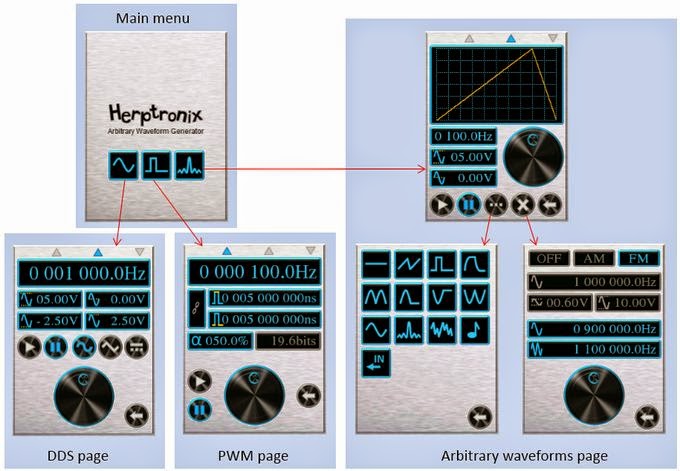
After a first quick & dirty attempt, I had to enhance the interface look; this one is working properly, but I admit that the old win95 look is really outdated. Moreover, there is a flickering issue on some widgets which are highly solicited (e.g. the frequency valueBox). The new interface is based on a brushed metal background, with dark widgets. I have also implemented the double buffering for the concerned widgets:


The new look is more modern (according to me; I’m not a graphic artist :s). The interface is still very reactive, but the memory footprint literally explodes (more than 90% of the flash memory is used). The user interface is composed of 4 “pages”:

- DDS (sinus/triangle waveform, with frequency / amplitude / offset control)
- PWM (PWM signal only)
- ARB (arbitrary waveforms & modulations)
- A menu page


Sinus / triangle waveform generation

These waveforms are directly generated by the AD9834, just by configuring its internal registers through the SPI bus. Nevertheless, a small detail shall be handled by the program: the frequency register is coded on 28 bits, split on two 16 bits registers. The access to the frequency register is not an atomic operation and shall be buffered first (through the FREQ0 / FREQ1 registers).

Arbitrary waveforms generation

I use the internal DAC of the AD9834 to generate these signals: this solution allows to keep the whole analog stage as is (same amplitude / offset control). For using the internal DAC, I configure the AD9834 with a triangle signal of 0Hz; then, I set the phase register to obtain the desired output voltage.

Some basic waveforms are available, such as saw tooth, exponential, noise, sin(x)/x… It is also possible to draw a waveform and play a wav file. However, there is a bandwidth issue: the AD9834 is accessed through a SPI bus, and even with a 20MHz clock, several microseconds are needed to send a single sample on the output. At the end, the microcontroller cannot provide more than 100kSPS (kilo Sample Per Second). Above this rate, the program is ran very slowly (most of the CPU time is spent into the ISR).

Go further

Even if this generator works properly, I have to admit that its electrical characteristics are closer to a gadget than a professional equipment (SNR below 45db). However, it would be easy to enhance its performances by modifying some components:

The DDS chip

A DDS such as the AD9102 is much more powerful than the AD9834; besides its more accurate DAC (14bits vs 10bits), its internal LUT can be reprogrammed: where the PIC32 can only provide 100kSPS, the AD9102 can provide up to 180MSPS (1800 time more). Unfortunately, this device is more expensive ($15/u at 100u) and is available only in LFCSP package (quite hard to solder).

The analog stage

The power supply should be changed first: the +/-7V coming from the buck regulators are obviously problematic (the output signal has some noise – 1.5MHz @10mVpp). A simple power supply based on a toroidal transformer and some 78xx / 79xx would be better. The LM7171 OPAMPs should also be changed by a more appropriate chip (a current feedback OPAMP for example).

DAC

The 10 bits of the AD5310 might not be the wisest solution for this application: for 10Vpp, 1LSB is equivalent to ~10mV, which is pretty good… if you use the whole range of the DAC! I reduced the range from 0-1023 to 0-920 due to the tolerance of the components, leading to an 11mV/LSB resolution. A 12 bits DAC would be a better solution here, thus a true voltage reference (the current one is derived from the 3.3V supply).[Link] Author: Philippe Duboisset


Tuesday, December 9, 2014

0

Simple Ac line Voltage Announcer Circuit Diagram

This is the Simple Ac line Voltage Announcer Circuit Diagram. The range of this simple ac-voltage monitor is 100 to 140 Vac, with a resolution of 1 V. The speech processor interprets an 8-bit binary input code from an analog-to-digital converter. The processor`s pulse-code-mod ulated output then passes through a filter and an amplifier before driving tbe circuit`s speaker to vocalize the corresponding number. Each time switch S1 is _pressed, the speech-processor program enun ciates tbe monitored voltage readings from 100 to 140 V, depending on the code at the input of a 27C64 EPROM. 

 Simple Ac line Voltage Announcer Circuit Diagram


Simple Ac line Voltage Announcer Circuit Diagram


The voltage-monitoring circuit consists of a bridge rectifier, filter capacitors, and a 10-Kilload resis tor. A divider, RA and RB, limits the input voltage to a maximum 2.55 V. The aid converter, IC4, then sends the voltage reading to tbe 27C64 EPROM, ICS. Pressing Sl sends a negative transient pulse to the write, WR, input of the aid converter, IC4, which initiates a 100-ttS conversion process. [Link]


Thursday, November 6, 2014

0

High Voltage Power Supply 10kV Circuit Diagram

This is smart High Voltage Power Supply 10kV Circuit Diagram. Be very carefull with this power supply because uses 220V mains and has 10KV at output. Characteristics: supply: 220V AC 50Hz mains Power: 15 Watts Ignition Voltage: 8KV .

High Voltage Power Supply 10kV Circuit Diagram

High Voltage Power Supply 10kV Circuit Diagram


Sourced By: Circuitsstream


Sunday, October 5, 2014

0

Simple Inverting Power Supply Circuit Diagram

This the simple electronic Inverting Power Supply Circuit Diagram. This circuit will provide a negative dc voltage that is approximately equal to the positive input voltage at no load and about 3 V less at 10 mA load. -`~ is from +5 to +15 Vdc. Do not exceed 15 V or Ul might be damaged. 

Simple Inverting Power Supply Circuit Diagram


Simple Inverting Power Supply Circuit Diagram


Thursday, March 6, 2014

0

Discrete Virtual Ground Circuit Diagram

Here is the simple virtual ground circuit based on discrete components. This simple design comes from miniaturization guru Sijosae. Is to make a buffer from generic discrete components. The transistors can be most any complementary pair of small-signal transistors. Suitable alternatives are the PN2222A and PN2907A. The diodes are generic small-signal types. An acceptable alternative is the 1N914. This circuit has better performance than a simple resistive divider virtual ground, and the parts cost is lower than for any other circuit mentioned here. It is, however, the least accurate of the buffered virtual ground circuits.

Discrete Virtual Ground Circuit Diagram

 
 Parts:

R1,R2 = 4.7K
R3,R4 = 4.7R
C1,C2 = 470uF-25V
C3,C4 = 47uF-25V
D1,D2 = 1N4148
Q1 = 2SC1384
Q2 = 2SA684
B1 = Battery


Wednesday, March 5, 2014

0

Stabilized Regulated Power Supply Circuit Diagram

This circuit of power supply, is very simple and easy to built, it can be assembled on a general-purpose PCB, finding its materials is very easy and cost-small. The output voltage is stabilized and is regulated in the region from 0V until + 15V dc, with biggest provided current 1 A. The regulation becomes with the P1. The Q1 is classic power transistor and it needs to be placed on a cool rib (Heatsink), when it works continuously in the region of biggest current it gets hot. The type of transformer is standard in the market.

Stabilized Regulated Power Supply Circuit Diagram


Parts:

P1 = 330R-Potentiometer
R1 = 560R-2W
C1 = 2200uF-35V
C2 = 100uF-35V
C3 = 10uF-25V
C4 = 220uF-25V
C5 = 100nF-63V
D1 = 18V-1.5W Zener
Q1 = 2N3055 NPN Transistor
T1 = 220VAC – 18V@ 1.5A
BR1 = 4x1N4007 Diode Bridge
SW1 = Mains On-Off Switch


Sunday, March 2, 2014

0

1.5 - 35 Volt DC Regulated Power Supply

Here is the circuit diagram of regulated power supply. It is a small power supply that provides a regulated voltage, adjustable between 1.5 and 35 volts at 1 ampere. This circuit is ready to use, you just need to add a suitable transformer. This circuit is thermal overload protected because the current limiter and thermal overload protection are included in the IC.

Picture of the circuit:

 1A 1.5 volt to 35 volt dc Regulated Power Supply Circuit Schematic
1A Regulated Power Supply Circuit Schematic
Circuit diagram:
 1A 1.5 volt to 35 volt dc Regulated Power Supply Circuit Diagram
1A Regulated Power Supply Circuit Diagram
Transformer selection chart:
  Transformer Selection Chart for 1A 1.5 volt to 35 volt dc Regulated Power Supply Circuit Diagram
Transformer selection Guide-Table For Power Supply
Parts:
IC = LM317
P1 = 4.7K
R1 = 120R
C1 = 100nF - 63V
C2 = 1uF - 35V
C3 = 10uF - 35V
C4 = 2200uF - 35V
D1-D4 = 1N4007

Features:
  • Just add a suitable transformer (see table)
  • Great to power your projects and save money on batteries
  • Suitable as an adjustable power supply for experiments
  • Control DC motors, low voltage light bulbs, …
Specifications :
  • Preset any voltage between 1.5 and 35V
  • Very low ripple (80dB rejection)
  • Short-circuit, thermal and overload protection
  • Max input voltage : 28VAC or 40VDC
  • Max dissipation : 15W (with heatsink)
  • Dimensions : 52x52mm (2.1” x 2.1”)
Technical Specifications
  • Input Voltage = 40Vdc max Transformer
  • Output Voltage = 1.5V to 35Vdc
  • Output Current = 1.5 Amps max.
  • Power Dissipation = 15W max (cooled)
Note:
  • It has not to be cooled if used for small powers. 28 Volt AC max is allowed for the input voltage.


Saturday, March 1, 2014

0

Simple Dual Voltage Power Supply 12 Volt

This is the simple circuit diagram of Dual Voltage Power Supply. It is used for Misc… application. This circuit is called regulated power supply. For this reason the main component of this circuit is Regulator IC. It also needs few components to built. The regulator 7812 is the positive voltage regulator and 7912 is the negative voltage regulator.

Simple Dual Voltage Power Supply 12 Volt Circuit Diagram


Simple Dual Voltage Power Supply 12 Volt


You can also use 7809 for 9 volt positive power supply and 7909 for negative voltage power supply. It regulates voltage from 24Volt to 12 Volt (DC). The transformer input is 110Volt to 220Volt (AC) and the output must be between 12Volt to 24Volt (AC) and current must be 500mA. In this circuit some capacitors are used as a filter for removing repole.


Tuesday, February 25, 2014

0

High LASER Power Supply

If you have ever worked with lasers, you know how fun and interesting it can be, you also know how expensive it can be. The high voltage power supplies for the laser tubes are often more expensive then the tubes themselves. This supply can be built with commmon parts, most of which you probably already have in your junk box. The secret is the transformer used. It is a common 9V 1A unit, connected backwards for step up. 
 
Please note that some people may have trouble with this supply. This is due to the slight difference in transformers.

CAUTION:LASER RADIATION

Schematic


This is the schematic of the laser power supply

Parts


Part

Total Qty.

Description

Substitutions
R1
1
10 Ohm 10W Or Greater Resistor
R2
1
Ballast Resistor, See "Notes"
D1, D2, D3
3
1N4007 Silicon Diode
C1, C2, C3
3
0.1 uF 2000V Capacitor
T1
1
9V 1A Transformer
S1
1
115V 2A SPST Switch
MISC
1
Case, Wire, Binding Posts (for output), Line Cord

Notes

1. T1 is an ordinary 9V 1A transformer connected backwards for step up.
2. R1 MUST be installed on a LARGE heatsink. A good heatsink is the metal case the supply is built in.
3. R2 Protects the laser tube from excess current. It should be soldered directly to the anode terminal on the tube. To find R2, start with a 500K 10W resistor and work down until the tube lights and remains stable.
4. If you have trouble with the tube not starting easily, use a longer anode lead that is wrapped around the tube.
5. Depending on the transformer you use, the circuit may or may not work. I cannot guarantee the operation of this circuit. Build at your own risk.


Monday, February 24, 2014

0

Made Dual Regulated Power Supply


Notes:
In this circuit, the 7815 regulatates the positive supply, and the 7915 regulates the negative supply. The transformer should have a primary rating of 240/220 volts for europe, or 120 volts for North America. The centre tapped secondary coil should be rated about 18 volts at 1 amp or higher, allowing for losses in the regulator. An application for this type of circuit would be for a small regulated bench power supply.


Saturday, February 22, 2014

0

Simple 0-30 VDC Stabilized power supply with current control 0.002-3 A

This is a high quality power supply with a continuously variable stabilised output adjustable at any value between 0 and 30VDC. The circuit also incorporates an electronic output current limiter that effectively controls the output current from a few milliamperes (2 mA) to the maximum output of three amperes that the circuit can deliver. This feature makes this power supply indispensable in the experimenters laboratory as it is possible to limit the current to the typical maximum that a circuit under test may require, and power it up then, without any fear that it may be damaged if something goes wrong.
There is also a visual indication that the current limiter is in operation so that you can see at a glance that your circuit is exceeding or not its preset limits.
 
 Technical Specifications - Characteristics
Input Voltage: ................ 24 VAC
Input Current: ................ 3 A (max)
Output Voltage: ............. 0-30 V adjustable
Output Current: ............. 2 mA-3 A adjustable
Output Voltage Ripple: . 0.01 % maximum

FEATURES
- Reduced dimensions, easy construction, simple operation.
- Output voltage easily adjustable.
- Output current limiting with visual indication.
- Complete protection of the supplied device against over loads and malfunction.
 
 How it Works
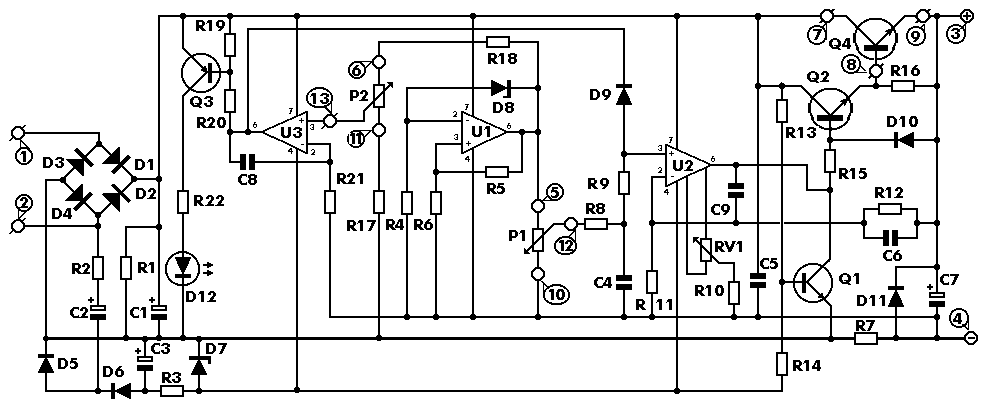
To start with, there is a step-down mains transformer with a secondary winding rated at 24 V/3 A, which is connected across the input points of the circuit at pins 1 & 2. (the quality of the supplies output will be directly proportional to the quality of the transformer). The AC voltage of the transformers secondary winding is rectified by the bridge formed by the four diodes D1-D4. The DC voltage taken across the output of the bridge is smoothed by the filter formed by the reservoir capacitor C1 and the resistor R1. The circuit incorporates some unique features which make it quite different from other power supplies of its class. Instead of using a variable feedback arrangement to control the output voltage, our circuit uses a constant gain amplifier to provide the reference voltage necessary for its stable operation. The reference voltage is generated at the output of U1. The circuit operates as follows: The diode D8 is a 5.6 V zener, which here operates at its zero temperature coefficient current. The voltage in the output of U1 gradually increases till the diode D8 is turned on. When this happens the circuit stabilises and the Zener reference voltage (5.6 V) appears across the resistor R5. The current which flows through the non inverting input of the op-amp is negligible, therefore the same current flows through R5 and R6, and as the two resistors have the same value the voltage across the two of them in series will be exactly twice the voltage across each one. Thus the voltage present at the output of the op-amp (pin 6 of U1) is 11.2 V, twice the zeners reference voltage. The integrated circuit U2 has a constant amplification factor of approximately 3 X, according to the formula A=(R11+R12)/R11, and raises the 11.2 V reference voltage to approximately 33 V. The trimmer RV1 and the resistor R10 are used for the adjustment of the output voltages limits so that it can be reduced to 0 V, despite any value tolerances of the other components in the circuit. Another very important feature of the circuit, is the possibility to preset the maximum output current which can be drawn from the p.s.u., effectively converting it from a constant voltage source to a constant current one. To make this possible the circuit detects the voltage drop across a resistor (R7) which is connected in series with the load. The IC responsible for this function of the circuit is U3. The inverting input of U3 is biased at 0 V via R21. At the same time the non inverting input of the same IC can be adjusted to any voltage by means of P2. Let us assume that for a given output of several volts, P2 is set so that the input of the IC is kept at 1 V. If the load is increased the output voltage will be kept constant by the voltage amplifier section of the circuit and the presence of R7 in series with the output will have a negligible effect because of its low value and because of its location outside the feedback loop of the voltage control circuit. While the load is kept constant and the output voltage is not changed the circuit is stable. If the load is increased so that the voltage drop across R7 is greater than 1 V, IC3 is forced into action and the circuit is shifted into the constant current mode. The output of U3 is coupled to the non inverting input of U2 by D9. U2 is responsible for the voltage control and as U3 is coupled to its input the latter can effectively override its function. What happens is that the voltage across R7 is monitored and is not allowed to increase above the preset value (1 V in our example) by reducing the output voltage of the circuit. This is in effect a means of maintaining the output current constant and is so accurate that it is possible to preset the current limit to as low as 2 mA. The capacitor C8 is there to increase the stability of the circuit. Q3 is used to drive the LED whenever the current limiter is activated in order to provide a visual indication of the limiters operation. In order to make it possible for U2 to control the output voltage down to 0 V, it is necessary to provide a negative supply rail and this is done by means of the circuit around C2 & C3. The same negative supply is also used for U3. As U1 is working under fixed conditions it can be run from the unregulated positive supply rail and the earth. The negative supply rail is produced by a simple voltage pump circuit which is stabilised by means of R3 and D7. In order to avoid uncontrolled situations at shut-down there is a protection circuit built around Q1. As soon as the negative supply rail collapses Q1 removes all drive to the output stage. This in effect brings the output voltage to zero as soon as the AC is removed protecting the circuit and the appliances connected to its output. During normal operation Q1 is kept off by means of R14 but when the negative supply rail collapses the transistor is turned on and brings the output of U2 low. The IC has internal protection and can not be damaged because of this effective short circuiting of its output. It is a great advantage in experimental work to be able to kill the output of a power supply without having to wait for the capacitors to discharge and there is also an added protection because the output of many stabilised power supplies tends to rise instantaneously at switch off with disastrous results.
 Construction
First of all let us consider a few basics in building electronic circuits on a printed circuit board. The board is made of a thin insulating material clad with a thin layer of conductive copper that is shaped in such a way as to form the necessary conductors between the various components of the circuit. The use of a properly designed printed circuit board is very desirable as it speeds construction up considerably and reduces the possibility of making errors. To protect the board during storage from oxidation and assure it gets to you in perfect condition the copper is tinned during manufacturing and covered with a special varnish that protects it from getting oxidised and also makes soldering easier.
Soldering the components to the board is the only way to build your circuit and from the way you do it depends greatly your success or failure. This work is not very difficult and if you stick to a few rules you should have no problems. The soldering iron that you use must be light and its power should not exceed the 25 Watts. The tip should be fine and must be kept clean at all times. For this purpose come very handy specially made sponges that are kept wet and from time to time you can wipe the hot tip on them to remove all the residues that tend to accumulate on it.
DO NOT file or sandpaper a dirty or worn out tip. If the tip cannot be cleaned, replace it. There are many different types of solder in the market and you should choose a good quality one that contains the necessary flux in its core, to assure a perfect joint every time.
DO NOT use soldering flux apart from that which is already included in your solder. Too much flux can cause many problems and is one of the main causes of circuit malfunction. If nevertheless you have to use extra flux, as it is the case when you have to tin copper wires, clean it very thoroughly after you finish your work.
In order to solder a component correctly you should do the following:
- Clean the component leads with a small piece of emery paper.
- Bend them at the correct distance from the components body and insert he component in its place on the board.
- You may find sometimes a component with heavier gauge leads than usual, that are too thick to enter in the holes of the p.c. board. In this case use a mini drill to enlarge the holes slightly. Do not make the holes too large as this is going to make soldering difficult afterwards.
- Take the hot iron and place its tip on the component lead while holding the end of the solder wire at the point where the lead emerges from the board. The iron tip must touch the lead slightly above the p.c. board.
- When the solder starts to melt and flow wait till it covers evenly the area around the hole and the flux boils and gets out from underneath the solder.
- The whole operation should not take more than 5 seconds. Remove the iron and allow the solder to cool naturally without blowing on it or moving the component. If everything was done properly the surface of the joint must have a bright metallic finish and its edges should be smoothly ended on the component lead and the board track. If the solder looks dull, cracked, or has the shape of a blob then you have made a dry joint and you should remove the solder (with a pump, or a solder wick) and redo it. Take care not to overheat the tracks as it is very easy to lift them from the board and break them.
- When you are soldering a sensitive component it is good practice to hold the lead from the component side of the board with a pair of long-nose pliers to divert any heat that could possibly damage the component.
- Make sure that you do not use more solder than it is necessary as you are running the risk of short-circuiting adjacent tracks on the board, especially if they are very close together.
- When you finish your work, cut off the excess of the component leads and clean the board thoroughly with a suitable solvent to remove all flux residues that may still remain on it.
connections
 (12,5cm x 8,7cm)
layout.
As it is recommended start working by identifying the components and separating them in groups. Place first of all the sockets for the ICs and the pins for the external connections and solder them in their places. Continue with the resistors. Remember to mound R7 at a certain distance from the printed circuit board as it tends to become quite hot, especially when the circuit is supplying heavy currents, and this could possibly damage the board. It is also advisable to mount R1 at a certain distance from the surface of the PCB as well. Continue with the capacitors observing the polarity of the electrolytic and finally solder in place the diodes and the transistors taking care not to overheat them and being at the same time very careful to align them correctly.
Mount the power transistor on the heatsink. To do this follow the diagram and remember to use the mica insulator between the transistor body and the heatsink and the special fibber washers to insulate the screws from the heatsink. Remember to place the soldering tag on one of the screws from the side of the transistor body, this is going to be used as the collector lead of the transistor. Use a little amount of Heat Transfer Compound between the transistor and the heatsink to ensure the maximum transfer of heat between them, and tighten the screws as far as they will go.
Attach a piece of insulated wire to each lead taking care to make very good joints as the current that flows in this part of the circuit is quite heavy, especially between the emitter and the collector of the transistor.
It is convenient to know where you are going to place every thing inside the case that is going to accommodate your power supply, in order to calculate the length of the wires to use between the PCB and the potentiometers, the power transistor and for the input and output connections to the circuit. (It does not really matter if the wires are longer but it makes a much neater project if the wires are trimmed at exactly the length necessary).
Connect the potentiometers, the LED and the power transistor and attach two pairs of leads for the input and output connections. Make sure that you follow the circuit diagram very care fully for these connections as there are 15 external connections to the circuit in total and if you make a mistake it may be very difficult to find it afterwards. It is a good idea to use cables of different colours in order to make trouble shooting easier.
The external connections are:
- 1 & 2 AC input, the secondary of the transformer.
- 3 (+) & 4 (-) DC output.
- 5, 10 & 12 to P1.
- 6, 11 & 13 to P2.
- 7 (E), 8 (B), 9 (E) to the power transistor Q4.
- The LED should also be placed on the front panel of the case where it is always visible but the pins where it is connected at are not numbered.

When all the external connections have been finished make a very careful inspection of the board and clean it to remove soldering flux residues. Make sure that there are no bridges that may short circuit adjacent tracks and if everything seems to be all right connect the input of the circuit with the secondary of a suitable mains transformer. Connect a voltmeter across the output of the circuit and the primary of the transformer to the mains.
DO NOT TOUCH ANY PART OF THE CIRCUIT WHILE IT IS UNDER POWER.
The voltmeter should measure a voltage between 0 and 30 VDC depending on the setting of P1, and should follow any changes of this setting to indicate that the variable voltage control is working properly. Turning P2 counter-clockwise should turn the LED on, indicating that the current limiter is in operation.
 Adjustments
If you want the output of your supply to be adjustable between 0 and 30 V you should adjust RV1 to make sure that when P1 is at its minimum setting the output of the supply is exactly 0 V. As it is not possible to measure very small values with a conventional panel meter it is better to use a digital meter for this adjustment, and to set it at a very low scale to increase its sensitivity.
 
 Warning
While using electrical parts, handle power supply and equipment with great care, following safety standards as described by international specs and regulations.
CAUTION
This circuit works off the mains and there are 220 VAC present in some of its parts.
Voltages above 50 V are DANGEROUS and could even be LETHAL.
In order to avoid accidents that could be fatal to you or members of your family please observe the following rules:
- DO NOT work if you are tired or in a hurry, double check every thing before connecting your circuit to the mains and be ready
- to disconnect it if something looks wrong.
- DO NOT touch any part of the circuit when it is under power.
- DO NOT leave mains leads exposed. All mains leads should be well insulated.
- DO NOT change the fuses with others of higher rating or replace them with wire or aluminium foil.
- DO NOT work with wet hands.
- If you are wearing a chain, necklace or anything that may be hanging and touch an exposed part of the circuit BE CAREFUL.
- ALWAYS use a proper mains lead with the correct plug and earth your circuit properly.
- If the case of your project is made of metal make sure that it is properly earthen.
- If it is possible use a mains transformer with a 1:1 ratio to isolate your circuit from the mains.
- When you are testing a circuit that works off the mains wear shoes with rubber soles, stand on dry non conductive floor
- and keep one hand in your pocket or behind your back.

- If you take all the above precautions you are reducing the
- risks you are taking to a minimum and this way you are protecting
- yourself and those around you.
- A carefully built and well insulated device does not constitute any danger for its user.
- BEWARE: ELECTRICITY CAN KILL IF YOU ARE NOT CAREFUL.
 
Check your work for possible dry joints, bridges across adjacent tracks or soldering flux residues that usually cause problems.
Check again all the external connections to and from the circuit to see if there is a mistake there.
- See that there are no components missing or inserted in the wrong places.
- Make sure that all the polarised components have been soldered the right way round. - Make sure the supply has the correct voltage and is connected the right way round to your circuit.
- Check your project for faulty or damaged components.
 

R1 = 2,2 KOhm 1W
R2 = 82 Ohm 1/4W
R3 = 220 Ohm 1/4W
R4 = 4,7 KOhm 1/4W
R5, R6, R13, R20, R21 = 10 KOhm 1/4W
R7 = 0,47 Ohm 5W
R8, R11 = 27 KOhm 1/4W
R9, R19 = 2,2 KOhm 1/4W
R10 = 270 KOhm 1/4W
R12, R18 = 56KOhm 1/4W
R14 = 1,5 KOhm 1/4W
R15, R16 = 1 KOhm 1/4W
R17 = 33 Ohm 1/4W
R22 = 3,9 KOhm 1/4W
RV1 = 100K trimmer
P1, P2 = 10KOhm  linear pontesiometer
C1 = 3300 uF/50V electrolytic
C2, C3 = 47uF/50V electrolytic
C4 = 100nF polyester
C5 = 200nF polyester
C6 = 100pF ceramic
C7 = 10uF/50V electrolytic
C8 = 330pF ceramic
C9 = 100pF ceramic
D1, D2, D3, D4 = 1N5402,3,4 diode 2A - RAX GI837U
D5, D6 = 1N4148
D7, D8 = 5,6V Zener
D9, D10 = 1N4148
D11 = 1N4001 diode 1A
Q1 = BC548, NPN transistor or BC547
Q2 = 2N2219 NPN transistor
Q3 = BC557, PNP transistor or BC327
Q4 = 2N3055 NPN power transistor
U1, U2, U3 = TL081, operational amplifier
D12 = LED diode


Social Time

Google Plus
Follow Us
Pinterest
Follow Us

Subscribe to our newsletter

(Get fresh updates in your inbox. Unsubscribe at anytime)