Video of the Day

Thursday, April 16, 2015

0

Simple Sensitive LPG Leakage Alarm Circuit Diagram

Here is an ultra-sensitive LPG sensor that generates loud beeps when it senses any gas leakage. It detects vapours of liquefied petroleum gas anywhere between 200 and 10,000 ppm and drives a piezobuzzer to catch attention for immediate action. The buzzer beeps until the concentration of gas in the air decreases to a safe level. The circuit uses an MQ6 gas sensor, which is designed to sense LPG, propane and isobutane gases.

Circuit and working
Fig. 1 shows the circuit of the LPG sensor. The circuit is built around 5V voltage regulator 7805 (IC1), gas sensor MQ6 (GS1), counter IC 4060 (IC2) and a few discrete components.


GS1 is a six-pin gas sensor that can detect very small traces of LPG in the air and has a swift response time. However, it has very less sensitivity to alcohol and smoke. The sensor’s output is in the form of resistance.

Component layout for the PCB

Fig. 1: Circuit of the sensitive LPG sensor

As indicated in Fig. 1, the pins of GSI are H, A and B, two each on either side. H pins are for the heater with no polarity. Input pins A or B and output pins A or B can be connected either way round.

The coil heater inside the sensor can be easily heated with 5V DC. If pin A is connected to 5V DC through variable resistor VR1, use pin B as the output or vice versa. Both A and B pins can be shorted. In short, H pins are connected to positive and negative rails, A or B pin to 5V DC, and B or A for output.

The resistance value of GSI is different for various kinds and concentration of gases. So when using this sensor, sensitivity arrangement is very important. For accurate detection, it is necessary to calibrate the sensor for 1000 ppm of LPG concentration in the air with load resistance of about 20 kilo-ohms. (In the datasheet, the load resistance range of MQ6 is mentioned as 10 kilo-ohms to 47 kilo-ohms.)


Fig. 2: An actual-size, single-side PCB for sensitive LPG sensor

Fig. 3: Component layout for the PCB

Preset VR1 is used to adjust the sensitivity of the sensor to a particular gas concentration. Output from the sensor is connected to the base of transistor T1, which acts as a switch to trigger the alarm generator built around IC2.

IC2 is a binary counter IC that oscillates using capacitor C2 and resistor R5. Transistor T1 controls the reset pin (pin 12) of IC2. When the reset pin is high IC2 does not oscillate, and when this pin goes low IC2 starts oscillating.

Working of the circuit is simple. When the sensor detects LPG in the air, its output becomes high and transistor T1 conducts to make reset pin of IC2 low. This triggers IC2 to oscillate, which is indicated by LED1. After a few seconds, the buzzer starts beeping to indicate gas leakage.

The circuit works off 12V DC from a battery (BATT.1) or you can use an adaptor. IC1 provides regulated 5V DC supply for the sensor and IC2.

 Construction and testing
An actual-size, single-side PCB for sensitive LPG sensor is shown in Fig. 2 and its component layout in Fig. 3. After assembling the circuit on a PCB, enclose it in a suitable case with an opening to allow the gas to enter. Place the unit near the LPG cylinder or gas stove within a distance of one metre. Vary preset VR1 to adjust the sensitivity of the sensor.

To test the circuit, check 12V at test point TP1 with respect to TP0 to verify the correct power supply. Place the unit near the gas stove burner and turn on the burner for a few seconds without igniting. Then, turn ’the burner ‘off’ and adjust VR1 until you see LED1 glowing. TP3 should be low at this moment.


Sourced By: EFY : Author Name :  D. Mohan Kumar


Sunday, March 22, 2015

0

What’s New in Spectrum Analysers

There are general-purpose spectrum analysers, and then there are specialised ones. What kind of a spectrum analyser do you need? The answer to this question basically depends on the maximum frequency range that you want to measure, after including the harmonics and intermodulation products of the wanted signals. Although you can get a lab-grade oscilloscope that can analyse low audio frequencies up to microwave, this is overkill if you are going to use it with audio equipment. On the other hand, if you are working on very high frequencies, you might need an analyser that has a resolution good enough to differentiate between the smaller frequencies.

N9344C handheld spectrum analyser

N9344C handheld spectrum analyser

Some new releases in this space are:
1. Tektronix MDO4000 mixed-domain oscilloscope, which is claimed to be the world’s first oscilloscope with built-in spectrum analyser.
2. R&S FSW-K91ac signal and spectrum analyser, which supports the new IEEE 802.11ac WLAN standard.
3. Anritsu MS2830A + OML MxxHWD, which has a  frequency coverage of up to 325 GHz.
4. Agilent N9344C HSA—an MIL PRF 28800 Class 2 compliant handheld spectrum analyser.
5. Scientech DSA800 Series spectrum analyser, which comes with a wide-screen display and is targeted at hobbyists.

The innovative lot includes:
1. Aronia X-Series USB RF spectrum analyser. Featuring specifications and performance similar to the equivalent Spectran handheld spectrum analysers, these RF spectrum analysers are controlled entirely via the USB interface using the real-time RF analysis software included with every unit.

2. Metageek WiSPY DBX—a pocket-sized tool designed for enterprise-level troubleshooting of WiFi environments. It has an amplitude range of –6.5 dBm to –100 dBm and amplitude resolution of 0.5 dBm. The device features an RP-SMA antenna too.

Purchasing an instrument for spectrum analysis being a major investment, make sure that you buy one that not only meets your today’s requirements but can also cope-up with the demands of tomorrow. With this in mind, selecting the ideal instrument should be a well-thought-out affair, with sufficient inputs from the people who are going to use it. Here are some pointers.

 1 Working with the IEEE 802.11ac WLAN standard?
If your project requires you to work with the upcoming 802.11ac WLAN standard, go for an analyser that is capable of analysing these signals. Although 802.11ac is still being defined, companies that chair the WiFi alliance have already brought out their own solutions using this standard.


The new standard requires 256 quadrature amplitude modulation (QAM), up to eight MIMO data streams, and a higher frequency band, along with wide bandwidths of up to 80 MHz. (The 160MHz bandwidth in this standard is achieved by using 80+80MHz mode.) Moreover, due to the 256 QAM, this standard requires an error vector magnitude (EVM) of -32 dB. The R&S FSW-K91ac tool features a very low EVM of less than -45 dB.


Announced on 20th June this year from Munich, the FSW-K91ac option enables the R&S signal and spectrum analyser to record and demodulate the full bandwidth of a WLAN signal in line with the new standard. It has a 31cm (12.1-inch) touchscreen with MultiView. MultiView provides users with simultaneous view of multiple measurements and applications. Pricing is available only on request.


 2 Spectrum analysers for education and hobbyists
Spectrum analysers for educational use and hobbyists should not only let them experiment with measurement testing but also act as a standard industrial instrument.


The DSA800 series from Scientech includes compact, light-weight and low-cost spectrum analysers that suit the education and hobbyist applications. The digital IF technology of this series helps in radio frequency (RF) applications like measurement of an RF amplifier’s characteristics, measurement of an RF bandpass filter’s characteristics, and measurement of voltage standing wave ratio.

The analysers offer a minimum resolution bandwidth of 100 kHz and are available with or without tracking generator. Their widescreen display, advanced measurement functions, electromagnetic interference (EMI) filter and quasi-peak detector kit, up to -135dBm displayed average noise level, phase noise of -80 dBc/Hz at 10kHz offset, total amplitude uncertainty of less than 1.5 dB, and the capability to interface through LAN, USB host, USB device and GPIB make them suitable for a majority of education and hobbyist applications.

The series comprises spectrum analysers to be used in basic electronics, basis communication, antenna and wireless communication labs.


 3 Millimetre-wave analysers
Millimetre-wave (mm-wave) analysers are intended for spectrum and signal analysis of emerging wideband communication systems. Using new capabilities, engineers can evaluate, characterise and manufacture products designed for emerging wideband standards, such as WiGig, including FCC Part 15 compliance emission testing requirements from 40 GHz to 200 GHz.


The MxxHWD harmonic mixer, based on a single-diode design, is available in waveguide bands from 26.5 GHz to 325 GHz. The harmonic mixer is a two-port frequency extension product with mm-wave interface for device-under-test (DUT) connection. The Anritsu MS2830A signal analyser, when coupled with the OML MxxHWD harmonic mixer, offers mm-wave frequency coverage from 26.5 GHz to 325 GHz.

 4 Radar, electronic warfare, EMI/EMC testing

Rapid advances in radar and electronic warfare technology have created the need for leading-edge testing technology and tools. Robust radar test equipment reduce uncertainty during the design process and deliver confidence in the integrity of increasingly complex designs.


Traditional signal analysers are unable to trigger on transient problems and the maximum available acquisition bandwidth in the mid-range is just 40 MHz.

To capture transients for analysis, Tektronix RSA5000 series offers frequency mask, frequency-edge, density, time-qualified and runt triggers. It can also be used to isolate hard-to-find hardware and software anomalies with cross domain triggering between multiple instruments. It can capture a seamless time record of RF frequencies into deep memory for up to 7 seconds at 85MHz bandwidth.


 5 Built for the field
For this kind of application, you require a spectrum analyser that is rugged, portable and performs well enough to get the job done. Compliance to MIL-PRF-28800 Class 2 is also important. This specification covers the general requirements for equipment used for testing and calibration of electrical and electronic equipment. The test equipment may be of commercial design and include general-purpose, special-purpose, peculiar, console-mounted, automatic test equipment and calibration standards.


The Agilent N9344C handheld spectrum analyser is built for the field. It features a channel scanner that can measure up to 20 channels simultaneously, as well as a spectrum monitor with spectogram display, record and playback. Moreover, it features AM/FM/ASK/FSK modulation analysis and time-gated spectrum analysis, which allows intermittent or burst signal spectrum measurement.

The Agilent N9344C is priced at ` 1,329,530 for the no-frills version, while a typical configuration would cost you ` 1,339,269.


Sourced By: EFY: Author name:  DILIN ANAND


Wednesday, March 18, 2015

0

Seven-Colour LED Lighting Circuit Diagram

Presented here is a simple circuit that uses six red, green and blue (RGB) LEDs to generate a running-light effect in seven colours—blue, green, red, cyan, yellow, magenta and white. The RGB LEDs have four pins, one for each colour and a common cathode. Different colours can be produced by mixing the primary colours (i.e., red, green and blue).

colours produced by three basic colours
Fig. 1: colours produced by three basic colours

Circuit and working
The circuit diagram for the seven-colour LED lighting is shown in Fig. 2. The circuit is built around timer NE555 (IC1), decade counter CD4017B (IC2), four-bit binary counter 7493 (IC3), driver IC ULN2003 (IC4), six RGB LEDs (RGB1 through RGB6), three BC547 transistors (T1 through T3) along with some basic components.

Seven-Colour LED Lighting Circuit Diagram
Fig. 2: Circuit of seven-colour LED lighting

The timer IC NE555 (IC1) is wired in astable multivibrator mode. It provides low-frequency clock pulses, the frequency of which is decided by timing components R1, VR1 and C2. The frequency of the timer can be varied using the preset VR1.

The output of IC1 at pin 3 is fed to decade counter CD4017B (IC2). IC2 has ten outputs, which go high in sequence when a source of pulses is connected to its CLK input (pin 14). Q0 through Q5 of IC2 are connected to IN1 through IN6 of IC4. Pin Q6 of IC2 is connected back to its reset pin 15 and input pin 1 of IC3 via diode D1. When Q6 pin of IC2 goes high, it resets IC2 and, at the same time, provides the high input clock to IC3 each time after the sixth clock of IC1.


IC3 is a four-bit binary counter, and its outputs QB through QD are connected to the bases of transistors T1 through T3 via resistors R21 through R23, respectively. The binary outputs of IC3 make corresponding transistors conduct and select a different colour after each cycle (see Table I).

The common-cathode pins of each RGB LED are connected to the outputs of IC4 as shown in Fig. 2. ULN2003 is used for driving these LEDs. You can add even more RGB LEDs in parallel to the existing ones to make a larger lighting system.

The working of the circuit is simple. When the circuit is switched on, the clock pulse is generated from pin 3 of the timer IC1, making outputs of IC2 high, sequentially, which decides the switching rate of LEDs that can be changed through VR1. The colours are selected by the binary output of IC3, which changes after every sixth pulse from IC1.


 A single-side PCB layout in actual size for seven-colour LED lighting circuit

Fig. 3: A single-side PCB layout in actual size for seven-colour LED lighting circuit

 component layout for the PCB

Fig. 4: component layout for the PCB

Construction and testing
A single-side PCB for seven-colour LED lighting is shown in actual size in Fig. 3, and its component layout is shown in Fig. 4. After assembling the circuit on a PCB, enclose it in a suitable case. You can wire LEDs the way you like and connect on the PCB. The circuit uses a 5V DC supply.


To test if the circuit is functioning properly, check the input supply at TP1 with respect to TP0. The output pulses generated by IC1 can be checked at TP2 with the help of an oscilloscope. The frequency of these clock pulses can be varied by VR1. The clock pulse to the binary counter IC3 can be checked at TP3.


Sourced By: EFY: Author : Riju Thazhathuveettil.


Thursday, February 26, 2015

0

Diplomatic Optical Burglar Alarm Circuit Diagram

This is the simple Diplomatic Optical Burglar Alarm Circuit Diagram. This optical burglar alarm uses two 555 timer ICs (IC1 and IC2). Both the ICs are wired as astable multivibrators. The first astable multivibrator built around IC1 produces low frequencies, while the second astable multivibrator built around IC2 produces audio frequencies. General-purpose Darlington photo-transistor T1 is used as the light sensor. To increase the sensitivity of the circuit, NPN transistor T2 is used.

Place phototransistor T1 where light falls on it continuously. Phototransistor T1 receives light to provide base voltage to transistor T2. As a result, transistor T2 conduct to keep reset pin 4 of IC1 at low level. This disables the first multivibrator (IC1) and hence the second multivibrator (IC2) also remains reset so the alarm (LS1) does not sound.


Diplomatic Optical Burglar Alarm Circuit Diagram


Diplomatic Optical Burglar Alarm Circuit Diagram


When light falling on Darlington phototransistor T1 is obstructed, transistor T2 stops conducting and reset pin 4 of IC1 goes high. This enables the first multivibrator (IC1) and hence also the second multivibrator (IC2). As a result, a beep tone is heard from speaker LS1. The beep rate can be varied by using preset VR1, while the output frequency of IC2 can be varied by using another preset VR2. This circuit works off a simple 6V-12V DC power supply.


PARTS LIST
Resistors (all ¼-watt, ± 5% Carbon unless stated otherwise)
R1, R5 = 1 KΩ
R2 = 100 KΩ
R3 = 4.7 KΩ
R4 = 10 KΩ
VR1 = 1 MΩ
VR2 = 100 KΩ
Capacitors
C1 = 1 µF/16V
C2 = 0.01 µF
C3 = 0.047 µF
C4 = 0.01 µF
C5 = 47 µF/25V
Semiconductors
IC1, IC2 = NE555
T1 = 2N5777 Photo Transistor
T2 = BC547
LED1 = RED LED
Miscellaneous
LS1 = 8Ω / 0.5W


Sunday, February 22, 2015

0

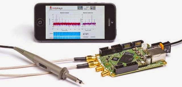
RED PITAYA

 RED PITAYA – An All-in-One Oscilloscope, Function Generator, Spectrum & Frequency Analyser 


A low cost, portable Control & Instruments device that claims to replace expensive lab and field instruments.

We are in the era of mobiles, gadgets and instruments that are portable, packed with lot of features, have web connectivity and available at a very economical price point. Pick up any electronic gadget or instrument and it will fit in this definition, so why should test and measurement instruments take a back seat!

Introducing RED PITAYA - an innovative single board, low cost, high spec, multifunctional and portable PCB based electronic Test & Measurement Device that aims to replace expensive lab and field instruments.

RED PITAYA – Open Source T&M Device

RED PITAYA – Open Source T&M Device

Features
RED PITAYA is a programmable device powered by Xilinx Zynq7000 SoC that combines dual core ARM & FPGA and runs on Linux. It uses open source ecosystem approach which let users to download standard applications from 'Bazaar' and customize these applications at various programming levels and also develop new applications using source code and documentation available from 'Backyard'.

It is an ideal platform for electronic enthusiasts, students and universities, HAM Radio operators and research institutes.


Red Pitaya In Action


Hardware Specifications of Red Pitaya

Inputs:-
1. The main inputs are two independent channels that run at 125MS/s with 14-bit resolution
2. Four low speed inputs, each at 100kS/s and 12-bit resolution.
Outputs:-
1. Two main analogue outputs at 125MS/s and 14-bit.
2. Four low speed outputs, each at 100kS/s and 12-bit resolution.

Expansion is possible via USB (to add a flash drive, WLAN adapter or camera for instance), and also via a connector that provides 16x FPGA pins for GPIO (e.g. for a custom add-on module). The instrument is typically accessed over Ethernet via a web interface and can be easily connected to local networks. Users can connect to it by simply writing its IP in the address bar for their browsers.

It is also possible to log in, execute remote commands and transfer data via SSH. A handy USB UART interface provides access to the SoC serial console for configuration and debugging.

Hardware Specifications of RED Pitaya


Standard Applications/Functionalities

Oscilloscope - 2 channels @ 125 MS/s 14 bit digital with external or signal based triggering capability
Spectrum Analyser - 2 channels with 50 MHz bandwidth signal with waterfall diagram capability
Arbitrary Waveform Generator - 2 channels @ 125 MHz 14 bit arbitrary waveform generation with external triggering capability

Frequency Response Analyser - 2 channels with 60 MHz bandwidth

The web interface enables access to Red Pitaya’s functionality from the majority of browsers. Applications are available on iPhone, iPad, other smartphones, tablets and PCs.

Software Functionalities, Programming
Red Pitaya can be customised for specific applications above its standard specification. It is based on GNU/Linux operating system and can be customised at different programming levels. Available software interfaces include:
- HDL
- C/C++
- Scripting languages
- Matlab
- HTML based web interfaces

Red Pitaya Target Audience
ELECTRONICS ENTHUSIASTS. Red Pitaya is a great springboard for electronics enthusiasts, because it offers great user interface and can be easily reconfigured for any kind of interaction with outside world by simply modifying the available applications. Out-of-the-box applications, such as oscilloscope or spectrum analyzer, enable fast debugging of electronic projects

STUDENTS. The learning process is simplified by Red Pitaya Backyard containing all the application's source code. Students can start programming by applying incremental changes to the code and publish their work in Bazaar and easily get in touch with a wide range of technologies and knowledge. It is also very appropriate for PhD or other research projects

TEACHERS & PROFESSORS. Red Pitaya is a compact replacement for several expensive instruments and also a universal teaching tool. It enables learning of WEB and embedded application programming, FPGA, signal processing, machine vision applications and it can be controlled by Matlab as well.

HAM RADIO OPERATORS. Amateur radio community uses a wide set of instruments such as SWR meter, network analyzer etc. Red Pitaya has a potential to replace them all. Besides that it can also be used as a radio station or software defined radio (SDR)

RESEARCH INSTITUTIONS. Red Pitaya is very suitable solution for detecting and analyzing fast phenomena, as well as generating or simulating complex signals.

To Conclude
RED Pitaya with its out-of-the-box features, applications & high spec caters to the requirements of all electronics professional working in different areas & on different applications that too at a very affordable price. It is not hard to believe that in coming days RED PITAYA with so much of distinguished features can become inseparable/invaluable device for any electronics lab, design house, R&D center, and university.


Sourced By: EFY:


0

Water-Level Indicator Schematic

Here’s a simple water-level indicator for overhead tanks that uses three LEDs (LED1, LED2, and LED3) to indicate minimum, middle, and maximum water levels in the tank.

The sensor probes comprise A, B, C, and D, where A is the common probe and B, C, and D are meant for sensing the minimum, middle, and maximum levels, respectively. When water in the tank touches sensor wires A and B both, a small current passes from A to B through water and to the base of transistor T1 via resistor R1. As a result, transistor T1 conducts, causing LED1 to glow. Similarly, when water touches sensor C, LED2 glows to indicate that the water has reached the middle level. Finally, when water touches sensor D, LED3 glows to indicate the maximum level of water. Thus all the three LEDs glow when the tank is full. At this stage, the motor should be switched off manually.


Water-Level Indicator Schematic


Water-Level Indicator Schematic


The circuit can be easily assembled on a general-purpose PCB and enclosed in a wooden box. The three LEDs should be mounted on the front panel of the box with a spacing of about 4 cm between them. Short lengths of four 18 SWG copper wires may be used for sensor probes. For the common sensor A, a bare copper wire of 18 SWG should be used. For sensors B, C, and D three single-core PVC wires should be used, with their insulation removed to a length of one centimetre towards the ends. All the four wires may be tied around a 12.5mm dia. PVC tube with nylon thread at different heights, without touching each other (not shown in figure).

The sensor probes should be kept in the tank vertically and connected to the main circuit using four flexible PVC wires of different colours.

The circuit is powered by a battery eliminator or a 6V battery and kept near the motor switchboard. The current drawn by the circuit, when all the LEDs glow, is up to 50 mA, which is less than the current drawn by a 6V bed-lamp.

The circuit costs around Rs 50.


Sourced y: EFY Author:  P. Venkata Ratnam


Tuesday, February 17, 2015

0

Simple 6V to 12V Converter Circuit Diagram

 This inverter circuit can provide up to 800mA of 12V power from a 6V supply. For example, you could run 12V car accessories in a 6V (British?) car. The circuit is simple, about 75% efficient and quite useful. By changing just a few components, you can also modify it for different voltages.

Notes

  • L1 is a custom inductor wound with about 80 turns of 0.5mm magnet wire around a toroidal core with a 40mm outside diameter.
  • Different values of D3 can be used to get different output voltages from about 0.6V to around 30V. Note that at higher voltages the circuit might not perform as well and may not produce as much current. You may also need to use a larger C3 for higher voltages and/or higher currents.
  • You can use a larger value for C3 to provide better filtering.
  • The circuit will require about 2A from the 6V supply to provide the full 800mA at 12V.


6V to 12V Converter Circuit Diagram


Simple  6V to 12V Converter Circuit Diagram


Parts
R1, R4 2 2.2K 1/4W Resistor
R2, R3 2 4.7K 1/4W Resistor
R5 1 1K 1/4W Resistor
R6 1 1.5K 1/4W Resistor
R7 1 33K 1/4W Resistor
R8 1 10K 1/4W Resistor
C1,C2 2 0.1uF Ceramic Disc Capacitor
C3 1 470uF 25V Electrolytic Capcitor
D1 1 1N914 Diode
D2 1 1N4004 Diode
D3 1 12V 400mW Zener Diode
Q1, Q2, Q4 3 BC547 NPN Transistor
Q3 1 BD679 NPN Transistor
L1 1 See Notes
MISC 1 Heatsink For Q3, Binding Posts (For Input/Output), Wire, Board


Sourced By:  circuitsdiagram-lab


Thursday, February 5, 2015

0

Brushless DC Motor Driver Circuit Diagram

Use of brushless DC motors (BLDCs) is on the rise. But their control usually requires rotor-position information for selecting the appropriate commutation angle. Normally, a Hall Effect sensor is used to sense rotor position. But in cost-sensitive applications, a sensor-less commutation scheme is often desirable. The circuit described here uses a DRV10866 driver IC to drive a small BLDC fan, without using any position sensors. A BLDC fan’s speed can be varied smoothly, without the usual steps associated with a normal AC fan.

Circuit and working
Fig. 1 shows the circuit of a sensor-less BLDC motor driver. The circuit is built around an NE555 (IC1), a DRV10866 (IC2) and a few other components.


Brushless DC Motor Driver Circuit Diagram

Fig. 1: Circuit of brushless DC motor driver

Fig. 2: An actual-size, single-side PCB for the brushless DC motor driver

Fig. 2: An actual-size, single-side PCB for the brushless DC motor driver
  
Fig. 3: Component layout for the PCB
 Fig. 3: Component layout for the PCB

DRV10866 driver IC from Texas Instruments is used to drive a small three-phase BLDC motor (M1). The circuit is of a three-phase, sensor-less motor driver with integrated power MOSFETs having drive-current capability up to 680mA peak. DRV10866 is specifically designed for low noise and low component-count fan-motor drive applications. A 150° sensor-less back emf scheme is used to control the three-phase motor.


A 100k pull-up resistor (R2) is used at pin 1 of IC2. Pins 2, 4, 7 and 6 of IC2 are connected to common, phase A, phase B and phase C of the BLDC motor, respectively. Pin 10 of IC2 is connected to pin 7 of IC1 to get the pulse-width modulated (PWM) signal from IC1 to control the speed of the BLDC motor.


The output signal (PWM) is available at IC1’s pin 7 (DIS) and not from the usual output pin 3 of the IC. The 25kHz (approx.) PWM signal’s duty cycle can be adjusted from 5% to 95% using potentiometer VR1. The speed of the BLDC motor can be controlled by varying the duty cycle of the PWM signal. Turning VR1 counter-clockwise lowers the duty cycle which, in turn, lowers the speed of the motor, and vice versa.

Construction and testing

An actual-size, single-side PCB for the brushless DC motor driver is shown in Fig. 2 and its component layout in Fig. 3. Assemble the circuit on the recommended PCB to minimise assembly errors. IC2 should be fitted on solder side of the PCB.

After assembling the components, connect a 5V DC supply to CON1 connector. To test the circuit for proper functioning, verify correct 5V supply for the circuit at TP1 with respect to TP0. Turn VR1 clockwise or counter-clockwise to increase or decrease the speed of the motor.


Author Name: Abhijeet Rai Sourced By: EFY


Sunday, January 25, 2015

0

Led Flasher Type of Police Circuit Diagram

This is the simple Led Flasher Type of Police Circuit Diagram. LED flasher same as that used in the police car, where the pace at which the lights flash is well paced and there is a sequence on each side. This type of flasher is also called strobe light or stroboscopic light. I began to develop a project to be published here, but by coincidence I ended up finding a circuit, easy to build and giving effect was wanting.

The electronic circuit flasher police is a Russian site, as the Russians have their own markup for semiconductor like this project, which uses KT815 transistors, for sure you will not find these transistors in a Western store, but of course are the replacements, in this case BD135.

Led Flasher Type of Police Circuit Diagram

Led Flasher Type of Police Circuit Diagram


Flasher LED Police type


This circuit is a classic of electronics, a flip-flop circuit, "astable multivibrators", this circuit is used for common flasher, but in this case two of this circuit were coupled to give the desired effect. The circuit flasher is so simple that can be done by a novice, as we see in the image below of the author, it was made on a standard printed circuit board.

How does the flasher Police

The flasher consists of two astable multivibrators, a leading astable formed by VT1 and VT2 transistors that generate the strobe and VT3 eVT4 transistors that have created short pulses to VT1 and VT2. The master oscillator is switched alternately strobe generator and the operating frequency of the generator is determined by the capacitors C1 and C4 and resistors R5, R6, R8 and R9.

You can use the trimpot R7 and R10 resistors to change the frequency of multivibrators, changing the frequency of blinking of the LEDs. The power transistors VT1 and VT3 and resistors R1 and R2 depend on the power of the LEDs used in the circuit.

Have the circuit power supply can be made with voltages 6-9 V, and its consumption is very low, enabling the use of batteries or battery. You can also change the operating voltage to 12 volts, just change some circuit resistors or put a 7809 regulator in input voltage.

Flasher LED type Police

I will give the most common equivalent found, the VT1 and VT2 transistors can be replaced by medium power transistors BD135, BD137 or BD139. The VT3 transistor can be replaced by transistors average power transistors BD136, BD138 or BD140.

But the transistor VT4 can be replaced by transistor 2sa611, BC556 or 2N4058 and other BCs of life. Below the video of the flasher police, the circuit can also be used for security systems, emergency flashing, holiday lighting, etc.


You can use higher power LEDs in this circuit since modify the resistors R1 and R2.


Friday, January 23, 2015

0

Simple Interface for Digital Sound Synthesis

You can make a digital sound synthesizer, for experimentation with sound equipment or with peripheral devices, using special integrated circuits or digital-to-analogue converters (DACs). But here is a simple 8-input digital sound-synthesis circuit for producing audio from digital codes that can be easily interfaced with microcontroller or microprocessor boards having up to eight TTL/CMOS-level digital output pins.

Circuit and working
Fig. 1 shows circuit diagram of the simple interface for digital sound synthesis. It is built around low-power audio amplifier LM386 (IC1), 9V voltage regulator 7809 (IC2) and a bridge rectifier (BR1).

Simple interface for digital sound synthesis
Fig. 1: Simple interface for digital sound synthesis


The 8-bit digital code (representing audio signal) input is applied at connector CON4. Resistors R1 through R8 and potmeter VR1 work as a simple DAC circuit. The relationships to get approximate values of resistors in the DAC are:

R1 = 2R2 = 4R3 = 8R4 = 16R5 = 32R6 = 64R7 = 128R8
Value of VR1 can be from 10% of R8 to 20% of R8.

The minimum value of each resistor (R1 through R8) depends on digital output levels. Capacitors C14 and C15, with switches S1 and S2 closed, filter the sound signals, and can be omitted, if not needed.


Fig. 2: An actual-size PCB layout for the circuit

The audio input is amplified by LM386 low-power amplifier. The gain is set to 200. With 9V power supply, the circuit outputs around 0.5W. The loudspeaker can be 4-ohm, but 8-ohm or higher is preferred to avoid overloading LM386.

The power supply is built around voltage regulator 7809 which gives a 9V regulated output. You can use 4-9V DC as external supply at CON7 input when 230V AC mains is not available.

Diode D1 is used for reverse protection of the regulator.

Construction and testing
An actual-size, single-side PCB for simple interface for digital sound synthesis (excluding the dotted box shown in the circuit) is shown in Fig. 2 and its component layout in Fig. 3. After assembling the circuit on a PCB, enclose it in a suitable plastic box.


Fig. 3: Component layout for the PCB

For testing, generate 1kHz square-wave signal and connect it to any input line of CON4 (D0 through D7). You will hear sound in the speaker connected at CON5.


You can write a simple software code, burn it into the microcontroller, connect its port pins to CON4 and check output from the speaker. You may change the code to various audio frequencies and check the output for experimentation.


You can also use this circuit as a simple audio signal mixer by applying the audio signals (including square-wave signals) at inputs D0 through D8.

Before using the circuit, do verify that voltages at test points are as per table.
The author was a researcher and assistant professor in Technical University of Sofia (Bulgaria) and expert-lecturer in OFPPT (Casablanca), Kingdom of Morocco. Now he is working as an electronics engineer in the private sector Bulgaria


Share on stumbleupon Share on gmail Share on facebook Share on twitter More Sharing Services


Sourced By:  EFY: Author Petre Tzv Petrov


Thursday, January 15, 2015

0

Tiny DDS - Open source DDS generator Project

This project is an open source (hardware & software) DDS generator, based on: smart TFT module, AD9834, LM7171 fast amplifier.

Description

The homemade function generator is a quite common project on the internet. We can find different ways to do it:

- The quick & dirty way based on a DDS module bought on eBay
- The analog version based on a MAX038 / XR2206
- The “clean” way based on a FPGA and a fast DAC (e.g. http://www.circuitben.net/node/14)
- The software way (e.g. Arduino + R/2R DAC)

From my side, I wanted a small one which could fits my needs without being too expensive. According to me, such generator should at least:

- Be easy to use
- Output a signal from 1Vpp to 10Vpp (+/-5V), from 0 to 1MHz
- Have a low profile
- Without electric hazard (shall work on a 12V DC)


Tiny DDS - Open source DDS generator Project Schematic

Tiny DDS - Open source DDS generator Project

Choosing the DDS chip
I first started to look for a cheap DDS chip on eBay; you have to be careful because most of DDS chips have only a sinusoidal output. Since I also want a triangular output, I have chosen the AD9834. According to its datasheet, this component is able to output a frequency of 37.5MHz from a clock of 75MHz… But do not expect a clean waveform at such frequency: without an internal PLL, this signal would be defined by only 2 points.

From my personal experience, I consider that a waveform shall be defined by 10-20 points to be well restituted. Relying on a 75MHz clock, the maximal output frequency would be 7.5MHz… This is not a very good performance for a professional equipment (even if the cheapest generators do not go above 4MHz), but it is quite reasonable for a hobbyist project.

The AD9834 can be found at $5 on eBay.

Amplitude control

The amplitude of the AD9834 can be controlled through different ways:

- Constant amplitude of 1Vpp (by default on most COTS), by wiring a resistor between the FS_ADJUST pin and the ground: this is quite annoying because an additional external amplifier will be need to set the amplitude to a desired level.

- Variable amplitude, by wiring a potentiometer between the FS_ADJUST pin and the ground: this solution is really easy to implement, but it will not allow a software management needed, for example, by the amplitude modulation.

- Software variable amplitude, by wiring a DAC to the FS_ADJUST pin. This solution is a bit more complex, but it will allow to implement some useful functionalities. I choose this way.

The amplitude will be set by the microcontroller of the smart TFT module (PIC32MX795). Unlike the other manufacturers (Atmel, ST…), Microchip did not include a DAC on their $10 chip… An external DAC is needed (an AD5310 found on eBay for $0.8 – 10 bit / SPI, SOT23-6 package). A small voltage divider is put between the DAC and the FS_ADJUST pin in order to transform the 0-3.3V of the DAC into 0-1.2V handled by the AD9834:


Notice: the logical levels are reversed: the minimal amplitude is reached when the DAC output is 3V3 and the maximal amplitude is reached when the DAC output is 0V.


AC coupling

The AD9834 generates a signal with a non-null offset, variable according to the amplitude. At this point, this offset is very annoying and shall be removed. Two possible ways:

- A high pass filter (a simple RC filter): this solution ensures an ideal AC coupling, but is problematic for the low frequency signals (a huge RC filter would be needed for frequencies below 100Hz)

- A differential amplifier: it is possible with the AD9834 because this component already has a differential output (IOUT / IOUTB pins). This solution makes the AC coupling effective even for very low frequencies, even for a DC signal. Therefore, the AC coupling will not be “ideal”: a small offset will be injected, and possibly some additional distortions due to the tolerance of the components (OPAMP & resistors). Nevertheless, it remains the best way according to me.


The ratio R15/R12 is set such as the maximal voltage outputted by U6 is +/-3.3V.

Offset control

Nothing difficult here: we just have to generate a DC signal between -3.3V and +3.3V. I use another AD5310 with a small OPAMP:


Notice: here again, the logical levels are reversed: the minimal offset is reached when the DAC output is +3.3V and the maximal offset is reached when the DAC output is 0V.

Final stage

Here, we have 2 signals: the one coming from the DDS (between -3.3V and +3.3V, AC coupled) and the one coming from the offset control (between -3.3V and +3.3V too). We just have to mix these 2 signals and amplify them to get a +/-5V output:


The LM7171 is able to output more than 100mA; nevertheless, the current is limited through a 100R resistor. A small LC filter is also implemented before the main output for filtering the 75MHz clock residual.

PWM output

Nothing complex here: a simple CMOS gate for buffering the PWM output of the microcontroller. I tried to use a fast comparator on the triangular output of the DDS, but the jitter was too important; I finally gave up this solution.


Analog input

Very minimalist… A simple resistor for limiting the input current, and a common Pi filter. The sampling frequency is not very high (~ 1KHz) because the internal ADC of the microcontroller is also used by the touchscreen inside an ISR.


Power supply / regulators

The generator is powered by a standard 12V plug. Some switching regulators produce the 5V (for the smart TFT module) and the +/-7V (used by the analog stage). The 3.3V comes directly from the smart TFT. The LT1616 are an expensive components on Farnell, but I found these on eBay for $0.8. Notice that any buck regulator should do the job here (+5V@200mA, +/-7V@200mA).

PCB

The whole schematic can be easily routed in a small PCB (smaller than a credit card). The PCB is composed of 2 layouts, with a common GND plan. The LM7171 shall be routed with care: due to its topology (fast OPAMP – 400MHz), a bad layout will make it oscillate. For this reason, I also add a footprint for a small 1pF capacitor: if the layout is not correct, I should be able to limit the oscillations with it.


Assembling the board

The PCBs (from SeeedFusion):


The finished board:


Assembled with the smart TFT:


Software

After a first quick & dirty attempt, I had to enhance the interface look; this one is working properly, but I admit that the old win95 look is really outdated. Moreover, there is a flickering issue on some widgets which are highly solicited (e.g. the frequency valueBox). The new interface is based on a brushed metal background, with dark widgets. I have also implemented the double buffering for the concerned widgets:


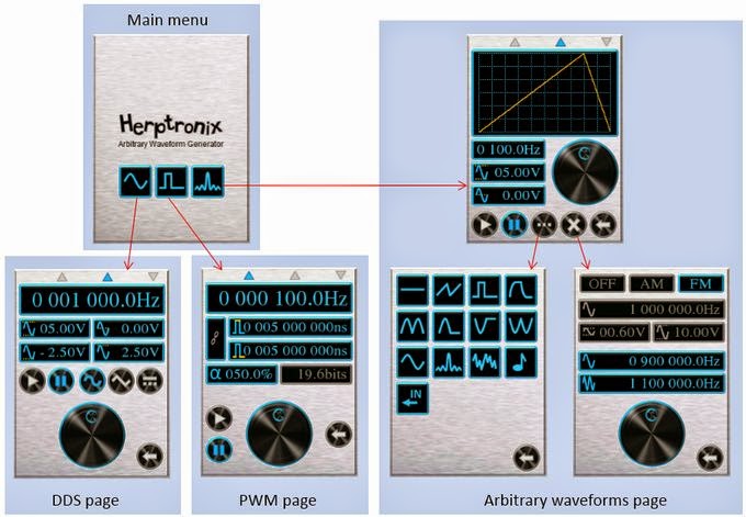
The new look is more modern (according to me; I’m not a graphic artist :s). The interface is still very reactive, but the memory footprint literally explodes (more than 90% of the flash memory is used). The user interface is composed of 4 “pages”:

- DDS (sinus/triangle waveform, with frequency / amplitude / offset control)
- PWM (PWM signal only)
- ARB (arbitrary waveforms & modulations)
- A menu page


Sinus / triangle waveform generation

These waveforms are directly generated by the AD9834, just by configuring its internal registers through the SPI bus. Nevertheless, a small detail shall be handled by the program: the frequency register is coded on 28 bits, split on two 16 bits registers. The access to the frequency register is not an atomic operation and shall be buffered first (through the FREQ0 / FREQ1 registers).

Arbitrary waveforms generation

I use the internal DAC of the AD9834 to generate these signals: this solution allows to keep the whole analog stage as is (same amplitude / offset control). For using the internal DAC, I configure the AD9834 with a triangle signal of 0Hz; then, I set the phase register to obtain the desired output voltage.

Some basic waveforms are available, such as saw tooth, exponential, noise, sin(x)/x… It is also possible to draw a waveform and play a wav file. However, there is a bandwidth issue: the AD9834 is accessed through a SPI bus, and even with a 20MHz clock, several microseconds are needed to send a single sample on the output. At the end, the microcontroller cannot provide more than 100kSPS (kilo Sample Per Second). Above this rate, the program is ran very slowly (most of the CPU time is spent into the ISR).

Go further

Even if this generator works properly, I have to admit that its electrical characteristics are closer to a gadget than a professional equipment (SNR below 45db). However, it would be easy to enhance its performances by modifying some components:

The DDS chip

A DDS such as the AD9102 is much more powerful than the AD9834; besides its more accurate DAC (14bits vs 10bits), its internal LUT can be reprogrammed: where the PIC32 can only provide 100kSPS, the AD9102 can provide up to 180MSPS (1800 time more). Unfortunately, this device is more expensive ($15/u at 100u) and is available only in LFCSP package (quite hard to solder).

The analog stage

The power supply should be changed first: the +/-7V coming from the buck regulators are obviously problematic (the output signal has some noise – 1.5MHz @10mVpp). A simple power supply based on a toroidal transformer and some 78xx / 79xx would be better. The LM7171 OPAMPs should also be changed by a more appropriate chip (a current feedback OPAMP for example).

DAC

The 10 bits of the AD5310 might not be the wisest solution for this application: for 10Vpp, 1LSB is equivalent to ~10mV, which is pretty good… if you use the whole range of the DAC! I reduced the range from 0-1023 to 0-920 due to the tolerance of the components, leading to an 11mV/LSB resolution. A 12 bits DAC would be a better solution here, thus a true voltage reference (the current one is derived from the 3.3V supply).[Link] Author: Philippe Duboisset


Sunday, January 11, 2015

0

Versatile Audio-Visual Alarm Circuit Diagram

This circuit uses an NE555 timer IC, some LEDs, a couple of piezo buzzers and a few other components to produce audio-visual effects as per your requirement. The timer NE555 and its equivalents are widely used for all sorts of audio and visual indications, such as door alarms. But the sound produced by these circuits may not be always pleasant to hear, or the light produced may not be visually appealing. With this circuit you can get different audio-visual effects.

Here we use LEDs for visual indication and buzzers for audible alarms as they require relatively low current to operate. By simply connecting some resistors and capacitors to NE555 we can obtain some interesting visual and audible effects as described here.

Circuit and working
Fig. 1 shows the circuit of the versatile audio-visual alarm which is built around timer NE555 (IC1), LEDs, buzzers and some resistors and capacitors. Resistors R1 and R2 and capacitor C1 determine the frequency of the LEDs’ blinking. The frequency is selected usually within the range of 0.1Hz to 20Hz, depending on your requirement. Values of resistors R1 and R2 can be above 1-kilo-ohm. Capacitor C1’s value can be between 1µF and 1000µF.

Versatile Audio-Visual Alarm Circuit Diagram

Fig. 1: The versatile audio-visual alarm circuit


Fig. 2: Actual-size, single-side PCB for the circuit

 Fig. 3: Component layout for the PCB


Timer NE555 drives two outputs, namely, Group1 and Group2. Group1 is built around resistors R4 and R6 along with LED1 through LED6. Group2 is built around resistors R7 and R8 along with LED7 through LED12.


Each of the groups can be configured to get different outputs. For example, in Group1 you can use only the LEDs (LED1 through LED3) connected to +12V, or only the LEDs (LED4 through LED6) connected to the ground, or both branches of these LEDs, or only piezo buzzer PZ1, or PZ1 with any combination of the LEDs, or you can omit the entire Group1.

The components in Group2 can form the same combinations as the components in Group1. The difference between the Group1 and Group2 is the use of resistor R5 and capacitor C2. These two components give light-decay effect to the LEDs and a pleasant low-pitch sound to piezo buzzer in Group2. Value of resistor R5 can be between 75-ohm and 1-kilo-ohm and that of capacitor C2 between 47µF and 1000µF.

At point 1 (TP2) in the circuit you can see a rectangular wave signal. At point 2 you can see a triangular or trapezoidal-like signal. The signals at points 1 and 2 should go low, almost to zero, and should go high, almost to 12V supply voltage.

Power supply used is 12V, but it can be in the range of 4.5V to 15V as well, depending on the number of LEDs used in each branch. Higher number of LEDs will require higher voltage. LED13 glows when power supply is connected in the circuit.

Resistors R4, R6, R7 and R8 are selected according to the number and type of the LEDs used. If the values of these resistors are too low, the output of the timer will be overloaded and the LEDs in the upper and the lower branches will get activated simultaneously.


Overloading may also damage the NE555 timer. It is suggested to keep the total output current drawn from NE555 below 100mA.

On/off switch S1 is used to start or stop the alarm. Connector CON2 is an optional input point for connecting a variable element, such as a preset, for adjusting or varying the frequency of the square signal for more audio-visual effects.

Construction and testing
An actual-size, single-side PCB for the versatile audio-visual alarm is shown in Fig. 2 and its component layout in Fig. 3. After assembling the circuit on PCB, enclose it in a suitable plastic box.

Connect piezo buzzers PZ1 and PZ2 at their provided places in the PCB. Also connect 2-pin terminal CON1 for power supply. Connect CON2 for external input (optional). Before using the alarm circuit, check at the test points given in the table.


Social Time

Google Plus
Follow Us
Pinterest
Follow Us

Subscribe to our newsletter

(Get fresh updates in your inbox. Unsubscribe at anytime)