Video of the Day

Thursday, June 22, 2017

0

IoT Based Notification System Using Android App

Presented here is a smart notification system for a door sensor, motion detector, fire alarm and doorbell using Raspberry Pi (RPi) and Pushover app. The project triggers an event through various sensors and sends notifications to your smartphone. Sensors used in this project include a magnetic reed switch for a door or window, PIR sensor for motion detection and NTC thermistor for fire alarm.

The issue of security is becoming more prevalent. The Internet of Things (IoT)-enabled home security solutions like this use sensors to collect and share data from multiple edge devices. If an attacker gains access to these smart systems through malicious means, the underlying functional logic of control systems can alert the owner. Connected home security systems offer a myriad of features including door and window sensors, motion detectors, fire alarms and so on, all connected via the Cloud to a mobile device or the Web.

Block diagram of the smart alert notification system using Android app is shown in Fig. 1.


Pushover app

Pushover is a service on the Web and an app for your phone or tablet that acts as a gateway for notifications. It can alert you to anything, including job postings, status of rain, emails from important people or a sensor activated in your home. Pushover lets you set up as many noise-free time periods as you like, using a feature called Quiet Hours. You can access alarm indications from anywhere in the world.
Circuit and working

Circuit diagram of the smart notification system using RPi is shown in Fig. 2. Hardware includes Raspberry Pi, Android phone, PIR sensor, reed switch, NTC thermistor, doorbell and a few other components.


Fig. 2: Circuit of the IoT based notification system using RPi

The PIR sensor connected across CON1 detects the presence of people through changes in infrared radiation from the human body in front of the door. It outputs around 3.3V high signal whenever it detects radiation change and correspondingly sends alert signals to your Android phone.

The magnetic reed switch connected across CON2 is usually installed on the frame of an exterior door or window. When the door or window opens, it moves away from the frame, magnetic field around the switch gets removed and corresponding alert signal is sent to your Android phone.

NTC thermistor connected across CON3 is used as the temperature-cum-fire sensor. Resistance of the NTC thermistor decreases with increase in temperature.

At room temperature, transistor T2 conducts. When temperature of the sensor goes above 70°C [depending on thermistor constant (K)], T2 stops conducting. When T2 stops conducting, an alert signal is generated in RPi, which is sent as a push message to the Android phone.

Most doorbells produce pulse-wave modulation waves while ringing. You need to hack the doorbell so that it produces at least 2V (pulse-wave modulation with low-pass filter) output signal. You may use this signal as an interrupt signal to drive RPi pin and generate an alarm log in your Android phone. Door-bell signal is fed to RPi through CON4.

When someone rings the doorbell, you will get a notification on your phone. Various alert notifications received on Android smartphone are shown in Fig. 3.

Software

Pushover makes it easy to get real-time notifications on your smartphone. Follow the steps given below to activate Pushover app on your Android device.

1. On your mobile device, open Pushover app and log into your account. You will be asked to register your device by providing a name for it.
 2. Visit https://pushover.net on your computer and log into your account. You should see your devices listed in a section called Your Devices, a little way down the page. Verify that the devices you have registered are on this list and are enabled.

3. Note down your user key (like, uyaa3u82r6rw853a2zhwj7afyxq4ba) as shown in Fig. 4. You will need it for your Python code.


Fig. 4: Typical user key generated on Pushover app

4. To get API key, click on Your Applications (doorbell) and note down your API token/key (like, au3kybdp4bmv3xs3qp1prku7pcrp9r) as shown in Fig. 5.


Fig. 5: Typical API key

5. Under Settings in Pushover, you can set an audio alert for quiet hours, etc for your mobile as per your requirement.

Testing Pushover app

Open Pushover app on your Android mobile. Open appliance.py file on the terminal in RPi. Change user_key and application_key in the code with your keys obtained as shown in Figs 3 and 4. Run the following command:

$ sudo python appliance.py

With the server connected to RPi, you will get ‘Appliance Server Started’ message in the terminal and ‘Appliance Started’ message on your mobile. As per the interrupt signal received from the input sensors (motion, door break, fire, doorbell, etc), the corresponding alert notification will be received on your Android phone through Pushover app.


Sourced By : EFY Author


Tuesday, June 20, 2017

0

Simple Bio-Feedback Circuit Diagram

Feed-back, means a reaction to a stimulus, I will explain, the concept is simple, but explanation is a bit troubled, bio-feedback is to electronically feed back a user through sound or Visual, it is possible to control your meditation state, causing the user to reach a pre-established state at any time.

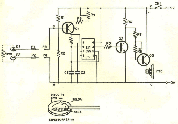
Simple Bio-Feedback Circuit Diagram

Simple Bio-Feedback Circuit Diagram


With this circuit it is possible to feedback from consciously varying the resistance of the skin, even though the equipment helps, even so will require training for this.

In order to use the biofeedback, the user must remain at rest, preferably lying down, since physical activity and variations of the emotional state influence the resistance of the skin, regardless of our will or unconsciously.

The biofeedback electrodes should be attached to the ring finger and index finger by tape or tape, and the hand should be in a comfortable, stationary position.

How Bio-Feedback Works

The biofeedback has as its main component an integrated circuit 555, configured as an astable multivibrator. The oscillation frequency of the 555 depends directly on the values of C1 and the collector current of Q1, which is connected as a current generator.

The resistors R1 and R2 attached to its base form a resistive divider which together with R3 and R9 determine the collector current of the transistor.

When the person connects the electrodes, the skin resistance is placed in parallel with R2, which changes the frequency of the oscillator. If skin resistance increases or decreases, we will see a drop or increase in the oscillation frequency of Cl1. R8 functions as volume control for Q3, which is the power amplifier.

Relation of Bio-Feedback Components

R1 – 47 kOhm x 1/4 Watt
R2 – 680 kOhm x 1/4 Watt
R3, R4, R6 – 1 kOhm x1/4 Watt
R5 – 22 kOhm x 1/4 Watt
R7 – 10 kOhm x 1/4 Watt
R8 – 50 kOhm – potentiometer linear
R9 – 10 kOhm – trimpot
C1 – 100 ηF pollster
C2 – 10 ηF pollster
CI1 – NE 555 ou equivalent
Q1 – BC 178 ou equivalent
Q2 – BC 549 ou equivalent
Q3 – 2N3055 ou equivalent
The biofeedback power is provided by a 9 Volt battery, but a well filtered source to avoid noise can be used without problems.
Source New Electronic Magazine 1 of 1977 - author of Gary Gronich.


Monday, June 19, 2017

0

Dual-Channel Active AC Analogue Probe Circuit Diagram

 This is a Dual-Channel Active AC Analogue Probe Circuit Diagram. It is suitable for oscilloscopes, multimeters and other analogue measurement equipment.

When experimenting with AM receivers for long, medium and short waves, users need a high-impedance analogue probe with input capacitance below 20pF. The required input impedance from the probe at low frequency is usually one mega-ohm or above.

Most of the low-cost passive probes for oscilloscopes have input capacitance well above 100pF. If you include the input capacitance of the oscilloscope, the total capacitance becomes even higher. The bandwidths of these low-cost passive probes are usually limited to 1-2MHz. These cannot be connected in parallel with L-C networks in AM receivers because that will change the parameters of these networks significantly.

Circuit and working

Fig. 1 shows the circuit diagram of the dual-channel, active AC analogue probe. It is built around two n-channel PN4393 JFET transistors (T1 and T2) and a few resistors and capacitors.
Dual-Channel Active AC Analogue Probe Circuit Diagram

Most of the oscilloscopes come with two channels, so you need a dual-channel active probe with common ground and common power supply.

At low frequency, the input resistance of the probe, determined mainly by resistors R3 and R4, is around 10-mega-ohm. At high frequency, the input impedance is determined by the total input capacitance of the probe. With careful implementation and use of appropriate JFETs, you can obtain input capacitance below 20pF.

Transistors T1 and T2 should have low noise level and low input capacitance. So you can choose from transistors like PN4391, PN4392 and PN4393 as these have input capacitance of typically 14pF. You can also use transistors J201, J202, J203, 2N5457, 2N5458 and BF245 (with 1.5dB noise figure). High-frequency JFETs in small cases are preferred but these are costly.

The voltage between the drain and the source of T1 and T2 is adjusted to around half of the power supply, using resistors R6 through R9 and jumpers J3 and J4. The circuitry using resistor R5, presets VR1 and VR2, and capacitor C3 is used to adjust the offset voltage applied to the gates of the JFETs. These components are not mandatory. If you choose not to use these, close jumpers J1 and J2, and connect resistors R3 and R4 to ground.

The gain of each of the channels is slightly below unity, but that is not important in most of the cases. Most oscilloscopes produce a square wave reference signal, which can be used for measurement of the gain and evaluation of the probe.

Construction and testing

An actual-size PCB layout for dual-channel active AC analogue probe is shown in Fig. 2 and its components layout in Fig. 3. After assembling the circuit on the PCB, enclose it in a suitable cabinet with connectors CON1 and CON2 affixed on the front side and connectors CON3 and CON4 on the rear side of the cabinet.

Actual-size PCB layout of dual-channel active AC analogue probe
 Actual-size PCB layout of dual-channel active AC analogue probe

 Components layout for the PCB

The probe can be implemented on a small PCB. During testing and adjustment, the inputs of the probe can be connected or soldered to L-C networks using very short (3-4cm long) conductors.

Power the circuit using a dry battery or rechargeable battery. The circuit does not require any special adjustment, so you can start using it straightaway after assembly. If you use jumpers J3 and J4, adjust VR1 and VR2 for the best performance of the probe.

After proper implementation, the probe can have bandwidths above 10MHz with a signal generator having low output impedance.


Sourced By :  EFY : Author Name : Petre Tzv Petrov


Friday, January 27, 2017

0

USB LED Night Light Circuit Diagram

A typical USB LED bulb shown in Fig. 1 is a 5V, 5W USB-powered solid-state lamp. At the heart of this light bulb is a circular aluminium PCB made with a bunch of 5730 SMD super-bright LEDs. Typical working voltage of a single 5730 SMD LED is in the range of 2.9V to 3.4V, and its current consumption is about 150mA. Fig. 2 shows some details of SMD LEDs used in the USB LED bulb. 


This gizmo inspired me to design a distinct USB LED night light with battery backup. Read More Click He


Wednesday, March 2, 2016

0

Simple Motion Detector Using NE555 Timer Circuit

This circuit is based on a passive infrared (PIR) sensor, which automatically switches on a device when someone comes close to it. It can be used for detection of theft or an unauthorised person entering a restricted area or building. It can also turn on lights when someone approaches the area where it is installed. Applications of this circuit include security systems, corridor lights and bathroom lights, among others.

Simple Motion Detector Using NE555 Timer Circuit
Fig. 1: Circuit diagram of the motion detector

Circuit and working

The circuit diagram of the motion detector using NE555 timer is shown in Fig. 1. It is built around 230V AC primary to 9V, 300mA secondary transformer X1, bridge rectifier DB107 (BR1), 6V voltage regulator 7806 (IC1), timer NE555 (IC2) and a few other components.


The 230V AC mains is stepped down to 9V, 300mA through step-down transformer X1. Secondary output of X1 goes to bridge rectifier BR1. Capacitor C1 filters the ripples and the rectified output is given to regulator 7806 (IC1). IC1 provides 6V regulated DC output to operate the circuit. LED1 is used as a power-on indicator.

 IC2 is configured in monostable mode. Time period of IC2 is based on resistor R4 and capacitor C3, which is around ten minutes in this case. By changing resistor R4 and capacitor C3 you can change the time period of IC2.

Output pin 3 of IC2 is connected to the base of relay driver transistor T2. Contacts of relay RL1 are connected to the load, which could be a CFL or a bulb connected across CON2.

The PIR sensor is a pyroelectric device developed for detection of human body infrared radiations. It has a single output that goes high when a valid motion is detected. That is, the load is switched on whenever the PIR module senses a body in motion nearby.

Under normal conditions, transistor T1 is cut off and collector output is high around 6V. When motion is sensed, output pin (OUT) of the sensor becomes high, making transistor T1 to conduct for a few seconds, and voltage at its collector goes low momentarily. This low signal triggers IC2. Output pin 3 of IC2 goes high for around ten minutes, energising relay RL1 through transistor T2, turning on the load for ten minutes.

In brief, when someone comes in front of the PIR module, its output triggers IC2 to turn on the load. Thereafter it is disabled automatically.


Fig. 2: Actual-size PCB of the motion detector


Fig. 3: Component layout of the PCB

Construction and testing
An actual-size, single-side PCB for the motion detector using NE555 timer is shown in Fig. 2 and its component layout in Fig. 3. Enclose the PCB in a box and install it at a suitable location. Connect the PIR module across CON1.

Connect transformer X1 to 230V AC mains. Verify various test point voltages as given in the table to ensure proper working before using the circuit.


Sourced By: EFY Author :  Kumar Abhisekh


Saturday, January 16, 2016

0

Simple Dual Audio-Signal Tracer Circuit Diagram

The circuit described here is of a dual audio-signal tracer. An audio-signal tracer is a simple device used to troubleshoot for audio signals in radio and other electronic circuitry.

The device is a battery-powered stereo amplifier with two loudspeakers, packaged into a small handheld unit with test probes. An optional diode detector can be incorporated for the detection of amplitude-modulated signals. A test signal (audio) is injected into the tracer at CON1/CON2 from various points of the circuit under test. So long as the signal is heard, the circuitry up to that point is (at least minimally) functional. However, if the signal disappears, a fault can be assumed to be present in the stage of the circuit just preceding it.

Simple Dual Audio-Signal Tracer Circuit Diagram
Fig. 1: Circuit diagram of the dual audio-signal tracer


The simple external diode detector is not only sensitive to amplitude modulation but even circuits that are normally used for other modulation schemes (such as FM radios) can be tested in some cases.

Circuit and working
Fig. 1 shows the circuit diagram of the dual audio-signal tracer. It is built around LM358 (IC1) and TDA2822M (IC2). LM358 has two independent, high-gain, internal-frequency-compensated operational amplifiers, which are designed specifically to operate from a single power supply over a wide range (3V to 32V) of voltages.


TDA2822M is a low-power stereo amplifier. Its outputs can be directly coupled with the speakers through decoupling capacitors. The tracer is sensitive enough to capture signals from most microphones.

The relatively-high input resistance of 1-mega-ohm (VR1 and VR2) makes it possible to capture audible signals from many tone-control circuits and filters. Input signals are applied to connectors CON1 and CON2 and amplified by the two amplifiers in IC1.

Both amplifiers (channels) are completely independent. Resistor R3 and diodes D2 and D3 protect the input of the first amplifier. Similarly, resistor R4 and diodes D4 and D5 protect the input of the second amplifier. Resistors R1 and R2, diode D1 and capacitor C1 provide the necessary bias DC voltage for the operational amplifiers in IC1.

Potentiometers VR1 and VR2 adjust the volume for the first and second channel, respectively. Op-amps of IC1 are configured as non-inverting amplifiers with gain fixed at ten. Voltage gains can have any values starting from one, depending on the need. However, it is not a good idea to have voltage gains higher than 30 because then the circuit becomes too sensitive to electromagnetic fields and may produce a lot of noise in the loudspeakers.

IC2 works as a dual-channel output amplifier. Each amplifier works with internally-fixed gain of around 100. The amplifier can drive loudspeakers and headphones with resistance equal to or higher than 8-ohm.


Fig. 2: An actual-size, PCB layout of the dual audio-signal tracer


Fig. 3: Component layout of the PCB

Construction and testing
An actual-size, single-side PCB of the dual audio-signal tracer is shown in Fig. 2 and its component layout in Fig. 3. After assembling the circuit on a PCB, enclose it in a suitable plastic box.

The circuit works well off 6V battery; the preferred power supply is 6V and above. The circuit is appropriate for the signal tracer, as general-purpose dual audio amplifier and as low-power stereo amplifier. The output power can reach 1W over 4-ohm with 9V power supply, which is more than enough for listening to the produced sound in a small room.


Sourced By: EFY Author


Sunday, January 10, 2016

0

Simple Motion Detector Using NE555 Timer

This circuit is based on a passive infrared (PIR) sensor, which automatically switches on a device when someone comes close to it. It can be used for detection of theft or an unauthorised person entering a restricted area or building. It can also turn on lights when someone approaches the area where it is installed. Applications of this circuit include security systems, corridor lights and bathroom lights, among others.

Simple Motion Detector Using NE555 Timer
 Fig. 1: Circuit diagram of the motion detector

Circuit and working

The circuit diagram of the motion detector using NE555 timer is shown in Fig. 1. It is built around 230V AC primary to 9V, 300mA secondary transformer X1, bridge rectifier DB107 (BR1), 6V voltage regulator 7806 (IC1), timer NE555 (IC2) and a few other components.

The 230V AC mains is stepped down to 9V, 300mA through step-down transformer X1. Secondary output of X1 goes to bridge rectifier BR1. Capacitor C1 filters the ripples and the rectified output is given to regulator 7806 (IC1). IC1 provides 6V regulated DC output to operate the circuit. LED1 is used as a power-on indicator.


IC2 is configured in monostable mode. Time period of IC2 is based on resistor R4 and capacitor C3, which is around ten minutes in this case. By changing resistor R4 and capacitor C3 you can change the time period of IC2.

Output pin 3 of IC2 is connected to the base of relay driver transistor T2. Contacts of relay RL1 are connected to the load, which could be a CFL or a bulb connected across CON2.

The PIR sensor is a pyroelectric device developed for detection of human body infrared radiations. It has a single output that goes high when a valid motion is detected. That is, the load is switched on whenever the PIR module senses a body in motion nearby.

Under normal conditions, transistor T1 is cut off and collector output is high around 6V. When motion is sensed, output pin (OUT) of the sensor becomes high, making transistor T1 to conduct for a few seconds, and voltage at its collector goes low momentarily. This low signal triggers IC2. Output pin 3 of IC2 goes high for around ten minutes, energising relay RL1 through transistor T2, turning on the load for ten minutes.

In brief, when someone comes in front of the PIR module, its output triggers IC2 to turn on the load. Thereafter it is disabled automatically.


Fig. 2: Actual-size PCB of the motion detector


Fig. 3: Component layout of the PCB

Construction and testing
An actual-size, single-side PCB for the motion detector using NE555 timer is shown in Fig. 2 and its component layout in Fig. 3. Enclose the PCB in a box and install it at a suitable location. Connect the PIR module across CON1.

Connect transformer X1 to 230V AC mains. Verify various test point voltages as given in the table to ensure proper working before using the circuit.


Sourced By: Efy  Author: Kumar Abhisekh


Monday, November 2, 2015

0

Bicycle USB Charger Circuit Diagram

This circuit has been developed to add a USB charging port to a bicycle for charging a mobile phone. The input supply for the circuit is produced by a dynamo (6V, 3W dynamo) in the bicycle. The circuit uses few components, which help in keeping the size, weight and cost of the unit down.

Circuit and working
The circuit is based on LM2596-5.0 (IC1). Its configuration, with minor changes, generally reflects the recommendations included in Texas Instruments’ datasheet of LM2596-5.0. The IC provides all active functions for a step-down (buck) switching regulator, capable of driving a 3A load with excellent line and load regulation.

The output of the regulator is 5V. It operates at a switching frequency of 150kHz, thus allowing smaller-sized filter components than what would be needed with traditional lower-frequency switching regulators. Fig. 1 shows the circuit diagram of the bicycle USB charger.

Bicycle USB Charger Circuit Diagram
Fig. 1: Circuit diagram of the bicycle USB charger
  
The alternating voltage generated by the dynamo is converted to DC by a full-wave bridge rectifier comprising Schottky barrier rectifier diodes D1 through D4 and a filtering electrolytic capacitor (C1). The output of the bridge rectifier, which is charged to peak value of AC voltage (nearly 10V), is input to switching regulator LM2596-5.0 to provide a regulated 5V (DC) output, which is suitable for charging mobile devices using the USB connector.

The 5mm LED (LED1) in the circuit indicates output status. Feedback connection FB (pin 4 on IC1) is connected directly to output voltage at electrolytic capacitor C2. As with all switching regulators, C2 should have a low ESR (equivalent series resistance) rating. Besides, 33μH inductor (L1) should be rated for a DC current of at least 1A. The dynamo output is connected to the circuit by switch S1.

Construction and testing
An actual-size, single-side PCB of the bicycle USB charger is shown in Fig. 2 and its component layout in Fig. 3. Assemble the circuit on the PCB in such a way that you can connect the mobile phone through a USB connector.

Fig. 2: Actual-size PCB layout of the bicycle USB charger


Fig. 3: Component layout of the PCB

LM2596 (IC1) is available in a standard TO-220 package as well as in a surface mount TO-263 package. The PCB layout is for TO-220 package. The whole circuit can be easily constructed even on a perforated prototyping board. The USB output is soldered directly in the prototyping board. However, it is very important to observe correct polarity when connecting the USB output socket. After construction and testing, enclose the unit in a suitable ABS/acrylic box.

Sourced By : EFY. Author T.K. Hareendran


Saturday, October 24, 2015

0

Simple Laser Based Security Lock Circuit Diagram

Presented here is a security system that uses an inexpensive laser torch which is usually available with a key ring. The advantage of this security lock is that you can use any laser torch or pointer that is easily available in toy shops. It employs minimal input keys and yet is very secure. It can be used as a door lock, briefcase lock or any other application related to an electronic locking system.

Circuit and working
The block diagram of a laser-based security lock is shown in Fig. 1 and its schematic diagram in Fig. 2. Switches S1 and S2 work as security input keys and switch S3 is used for opening the lock manually. The lock can be an electric strike installed on the door frame to allow access with an access control system or any electronic remote control system.


Fig. 1: Block diagram of the laser based security lock

Electric strikes are generally available in two configurations—fail-secure and fail-safe. In fail-secure configuration, applying electric current to the strike causes it to open; whereas in fail-safe configuration, applying electric current to the strike causes it to lock. A fail-secure configuration is used in this project.

Opening the lock. The use of switch S2, pressing and releasing of switch S1 and supplying the laser pulses at the right time are the security features of this circuit. Switch S2 should not be released during the entire operation, otherwise the counter will get reset and you will not be able to open on the lock.

Circuit diagram of the laser based security lock
Fig. 2: Circuit diagram of the laser based security lock


When switch S1 is pressed, the first in-built timer of IC2 is triggered. Its output pin 5 goes high for four seconds. LED1 glows and transistor T3 conducts. During this time, the collector of T3 becomes low, which in turn pulls the clock enable pin (pin 13) of IC1 to low state. This enables the counter (IC1) to count. During this time, five laser pulses are applied (by you) at photo sensor T1. These signal pulses go to clock pin 14. LED4 glows and T2 conducts at the fifth pulse. This triggers the in-built second timer of IC2. Its output pin 9 goes high for two seconds. The high state is indicated by the glowing of LED2. When LED2 goes off, you press switch S1 and release it. The first timer is triggered again and its output is high for four seconds. During this time, you send another five pulses of laser beam towards the sensor. At the fifth pulse, LED3 glows and transistor T4 conducts. This action triggers IC3 and its output pin 3 goes high for ten seconds. That is, the lock opens for ten seconds.
 The lock driver circuit is connected to output pin 3 of IC3. The circuit is powered off a 5V DC supply. Normally the electric lock or electric strike works off a 12V DC. To make the circuit simple, the lock driver section is not shown here.

Construction and testing
An actual-size, single-side PCB layout of the laser-based security lock is shown in Fig. 3 and its component layout in Fig. 4.

Mount the components on the PCB to avoid any assembly errors. Enclose the circuit in a suitable box. Mount switches S1, S2 and S3 at appropriate locations. If the circuit is to be used as a door lock, photo sensor T1, switches S1 and S2 should be mounted outside the door frame. The photo sensor should be enclosed in the box with a suitable contraption so that it can receive the laser beam properly. Switch S3 should be installed on other side of the wall near the door frame.

 An actual-size PCB layout for the laser based security lock circuit
 An actual-size PCB layout for the laser based security lock circuit  


 Component layout of the PCB 

While pressing switches S1 and S2 simultaneously, point the laser torch toward the photo transistor sensor T1 and press on/off button of the laser torch five times within four seconds. Release switch S1 while pressing switch S2. Wait for two seconds till LED2 goes off. Keeping S2 pressed, press S1 and release it, press on/off button of laser torch five times again. The lock will open for ten seconds and then close automatically. The lock can also be opened from the inside (for ten seconds) by pressing switch S3.

Sourced by : EFY


Thursday, September 3, 2015

0

Simple Adjustable Staircase Waveform Generator

Staircase signals find many applications in the field of electronics, such as in television systems, telemetry, and analogue and digital communications. Here is a circuit illustrating the basic principles of staircase waveform generator. Advantages of this circuit are: simple, low-cost, no complex programming, easy-to-assemble on a breadboard and adjustable staircase waveform outputs of variable step sizes and durations.

Circuit and working
The circuit diagram of a simple adjustable staircase waveform generator is shown in Fig. 1.

IC1 (74HC14) is a hex inverter Schmitt trigger that generates oscillatory pulse (square wave) and gives an output clock at pin 14 of IC2 (74HC93), which is a 4-bit binary ripple counter. Pins 8, 9 and 12 of IC2 are connected to select pins of IC3 (74HC4051), which is an 8-channel analogue multiplexer/demultiplexer with three digital selected pins 9, 10 and 11. Input pins of IC3 are connected to eight potentiometers of 10-kilo-ohm each.


Variable step sizes are obtained by varying these potentiometers. Depending on the selected pins and values of potentiometers, we get different types of staircase waveforms at output pin 3 of IC3. When these waveforms are further given to the input pins of IC4 (dual op-amp), it simply buffers them. Fig. 2 shows four different types of staircase output waveforms obtained at CON5.

 Fig. 1: Circuit diagram of simple adjustable staircase waveform generator


Fig. 2: Staircase output waveforms

Vcc depends on the ICs used in the circuit and can be 5V. With CMOS ICs like 74Cxxx and CD4000B, we can use Vcc up to 15V.

Construction and testing
An actual-size, single-side PCB layout of the simple adjustable staircase waveform generator is shown in Fig. 3 and its component layout in Fig. 4.

The frequency at pins 1 and 2 of IC1 depends on the type of IC used and values of capacitors and resistors connected to gate N1 of the IC. It can be from 1Hz to 1MHz. If you use an external frequency, move S1 to position 5 to bypass capacitors C1 through C4.

Switch S2 selects the source of reference voltage for VR1 through VR8. In the first position (1), Vcc is used as reference source. In the second position (3), signal from connector CON3 is used as reference source.

Fig. 3: An actual-size PCB layout
   
 Fig. 4: Component layout of the PCB


The fixed-amplitude staircase output waveform is obtained at CON5 and variable-amplitude staircase waveform is obtained at CON6.


Each waveform consists of eight clock pulses, zero through seven. The height of each step is adjusted according to the need using potentiometers VR1 through VR8. The frequency of the step is determined by the oscillator around gate N1 of IC1 or by the external clock signal applied to connector CON1. For troubleshooting, check the various test points and ensure you get the outputs as per table.


Sourced by : EFY : Author Petre TZV Petrov


Sunday, August 16, 2015

0

Sequential Tilt-Motion Lock

Here is a project for locking and unlocking with a tilt sensor by tilting it in a defined sequence. It uses an accelerometer module to detect the tilt motion. If the sequence matches with the predefined motion sequence, the lock opens. You can build this lock for a briefcase, ballot box, portable cashbox or even as a door-lock using suitable mechanical arrangement.

Circuit and working
Fig. 1 shows circuit diagram of the sequential tilt-motion lock. The circuit is built around Arduino Uno board (Board1), accelerometer module (ACC.1), solenoid lock/electric strike and a few other components.

Circuit diagram of sequential tilt-motion lock
Fig. 1: Circuit diagram of sequential tilt-motion lock

Arduino Uno board. Arduino is an open source electronics prototyping platform based on flexible, easy-to-use hardware and software. It is intended for artists, designers, hobbyists and anyone interested in creating interactive objects or environments.
Arduino Uno is a board based on ATmega328 microcontroller. It consists of 14 digital input/output pins, six analogue inputs, a USB connection for programming the on-board microcontroller, power jack, an ICSP header and a reset button. It is operated with a 16MHz crystal oscillator and contains everything needed to support the microcontroller. It is very easy to use as the user simply needs to connect it to a computer with a USB cable, or power it with an AC-to-DC adaptor or battery to get started. The microcontroller on the board is programmed using Arduino programming language and Arduino development environment.

Pins A0, A1, A2, A3, A4 and A5 of Board1 are connected to pins ST, Z-axis, Y-axis, X-axis, GND and Vcc of the accelerometer module, respectively. Pin 10 of Board1 is connected to solenoid driver transistor through which the solenoid lock is connected.

Accelerometer module. An accelerometer is an electromechanical device that measures acceleration. The accelerometer module used here is based on ADXL335 triple-axis accelerometer from Analog Devices. The sensor has a full sensing range of ±3g.

The microcontroller in Board1 receives data at pins A1, A2 and A3 for z, y and x axes, respectively, from the accelerometer. This data is continuously compared by Board1 with predefined values for each axis. If the received sequence matches, Board1 unlocks the lock, which is either a solenoid lock or any other suitable magnetic lock. (We used a 12V electric strike for testing.) Glowing of LED1 indicates that the lock is open.

Software
The software for this project is written in Arduino programming language. The Arduino Uno is programmed using Arduino IDE software. ATmega328 on Arduino Uno comes with a boot loader that allows you to upload new code to it without the use of external hardware programmer. It communicates using the STK500 protocol. You can also bypass the boot loader and program the microcontroller through in-circuit serial programming (ICSP) header, but boot loader programming is quicker and easier. Select the correct board from ‘Tools → Board’ in Arduino IDE and burn the program (sketch) through standard USB port in the computer.

Fig. 2: An actual-size PCB layout for the sequential tilt-motion lock

Fig. 3: Component layout for the PCB


Construction and testing

An actual-size (Arduino shield type), single-side PCB for the sequential tilt-motion lock is shown in Fig. 2 and its component layout in Fig. 3. Assemble the circuit on the recommended PCB to minimize assembly errors.

To test the circuit for proper functioning, switch on S1 and verify correct 12V supply for the circuit at TP1 with respect to TP0.

The neutral position of accelerometer module is parallel to the earth’s surface. The +Y and +X axes are marked on the accelerometer module. The default tilt sequence of this circuit defined in the source code is -X, -Y, -X, +Y, -Y. If the tilt sequence is correct, you can observe the glowing of an in-built LED (not shown here) connected to pin 13 of Arduino board. If you want to change the sequence, change it in the source code, recompile the program and burn into the microcontroller.

To open the lock, switch on S1 and tilt the circuit sequentially, as mentioned above, within one minute. If correct action is not completed within one minute, you need to repeat the tilt sequence from the start to unlock it. To close the lock, just switch off the circuit using on/off switch S1.


Soueced By : EFY Author:  Akhil Kaushik


Saturday, August 8, 2015

0

12V, 1A SMPS Circuit Diagram

Most electronics enthusiasts require DC power supplies to operate various devices and accessories. The most popular and common supply is a 12V DC supply that can be easily derived from the household AC supply with transformation, rectification, filtering and stabilisation. These power supplies have a bulky steel- or iron-laminated transformer that provides a safety barrier for the low-voltage output from the AC input, and reduces the input from typically 230V AC to a much lower voltage. The low-voltage AC output from the transformer is then rectified by two or four diodes and smoothed into low-voltage DC by large electrolytic capacitors.


Fig. 1: The author’s prototype

A switched mode power supply (SMPS) offers the same end results at a lower cost and higher efficiency. For a given output power, an SMPS is lighter and smaller. This is because, if the frequency of operation is increased, one can get away with using a smaller core cross-sectional area. Besides, an iron-core transformer works only up to about 10 kHz, and if we need something in 50-100kHz range, we need a ferrite core.


Circuit and working

Fig. 2 shows the circuit of a simple 12V, 1A SMPS. The circuit is built around a low-power offline switcher TNY266 (IC1), photo-transistor photo-coupler EL817 (IC2), a flyback transformer (X1) and some other easily-available components.

Low-power offline switcher (TNY266). The SMPS here has been designed using a TNY266 chip, which is affectionately called the ‘555’ of SMPS. This device has a 700V power MOSFET, an oscillator, a high-voltage switched current source, a current limiting and thermal shutdown circuitry integrated onto a monolithic device. The start-up and operating power is derived directly from the voltage on the drain (pin 5), eliminating the need for a bias winding and associated circuitry. In addition, the device incorporates auto-restart, line under-voltage sense, and frequency jittering.

The drain-source breakdown voltage of the MOSFET in TNY266 is important. During the ‘off’ period, the MOSFET sees rectified 317V DC approximately. Additionally, it sees the reflected voltage of the secondary, which is about 130V AC. It also encounters the ringing voltage from the leakage inductance, and the drain-source capacitance of the MOSFET. Therefore a MOSFET with a Vdss of 650V DC is expected to keep the necessary safe operating margin. Fortunately, a MOSFET with these properties is included in TNY266.

The 230V AC input is connected at CON1, which is rectified by diode D1. The neon lamp (NL1) glows when the input supply is present. Resistor R1 limits the current through the lamp. The rectified output goes to the first terminal (A) of coil L1 and the second terminal (B) is connected to the drain of the inbuilt MOSFET in IC1. Diodes D2 and D3 are essentially the snubbers, and are used to protect the MOSFET from going above 600V.

Flyback transformer. A flyback circuit is simply a pair of coupled inductors. If a current is passed through one inductor, it will store energy E = ½ (L.I2), where ‘L’ stands for inductance in henry, and ‘I’ for current in amperes. This energy can later be taken out of the second inductor, which is coupled to the former at a different volt-current ratio. The flyback’s energy storage and extraction mechanism is interesting. The key point is the polarity of the winding; the secondary is out of phase with the primary, as is evident in Fig. 2 (the dots indicate polarity).

12V, 1A SMPS Circuit Diagram

Fig. 2: Circuit of the 12V, 1A SMPS


Fig. 3: An actual-size, single-side PCB for the 12V, 1A SMPS


Fig. 4: Component layout for the PCB

When the MOSFET of IC1 is ‘closed,’ the current flows through L1. Point A on L1 goes positive and by transformer action, and considering the polarity of dots, point C on L2 goes negative. This reverse biases diode D4, and no current flows in the secondary winding. Similarly, when the MOSFET is ‘open,’ the current flow through L1 is interrupted and, by Lenz’s Law, a voltage of polarity opposite to the applied voltage appears on L1 and L2. Thus, point A on L1 goes negative and point C on L2 goes positive. This situation forward biases diode D4. The energy stored in the core causes the current to flow through winding L2. This charges capacitor C2 and also powers the load. The charge on C2 is used in the next half of the cycle to keep the current through the load somewhat constant. The cycle repeats endlessly. The MOSFET is switched on/off continuously at a frequency of around 120 kHz to keep this process running.

The design data for the transformer is as follows:
1. Duty cycle = 0.45 (max. duty cycle for DCM flyback = 0.5; less 10% safety margin)
2. Core saturation magnetisation Bsat = 0.24T
3. Core area of EE20 = 25mm2

Winding details computed for the SMPS are shown in Table I.

The feedback circuit. Regulated output needs feedback to control the pulse width modulation (PWM) of the MOSFET. TNY266 has a fabulous control feature; it stops the switching cycle as soon as any current is taken out of pin 4 of the device. If SMPS output exceeds the zener break-down voltage then ZD1 conducts. This lights the opto-LED and the opto-transistor grounds pin 4 of IC1, resulting in immediate stoppage of the switching cycle. Also, when the primary is conducting, diode D4 on the secondary side is reverse biased. At this time, if the voltage across D4 exceeds its reverse breakdown voltage, the SMPS will fail. Here we have used an SB160 Schottky diode with breakdown voltage= 60V.

Connector CON2 provides 12V regulated DC supply.

Construction and testing
A general core-selection ‘rule of thumb’ for SMPS below 50 watts is 2-3 mm2 core area per watt. For a primary input power of 16W, a core with a core area of 32-48 mm2 is needed. EE20 core will work well for this design.

Transformer wire. Any wire that can carry the required current can be used. To know how much current a given wire can carry, SMPS designers use a number called current density [J] for this calculation. Empirically, a good starting point is J = 5 amps/mm2. The primary carries 0.3 amps, so it can be wound using SWG 38. The secondary carries 5 amps, so it can be wound with SWG 26. A good practice would be to wind the secondary using two parallel strands of SWG 28. This reduces the skin effect. The key problem in flyback transformers is leakage inductance, which is caused by poor coupling between the primary and secondary windings. So wind them tight, with full overlap.

The air gap. Flybacks made from power ferrites must have an air gap. The energy stored in a flyback primary is E = ½ L.I2. Peak primary current depends inversely on primary inductance. An air gap increases the energy storage capacity of a flyback transformer. It is calculated as follows:
Air gap = (µ0 x N2 x Ac)/Lprimary
where:
µ0 = permeability of free space, 4π x 10-7
Ac = Core area (m2)
N = Primary turns
Lprimary = (Vprimary.pk × Ton.primary)/ Iprimary.pk

The primary inductance computes to ~3mH, so the air gap is approximately 0.2mm. However, this value is not critical, as was experienced by the authors during their experiments. Any air gap in the neighbourhood of the calculated value works well. A thin sheet of plastic or paper works fine.

An actual-size, single-side PCB for the simple 12V, 1A SMPS is shown in Fig. 3 and its component layout is shown in Fig. 4. Assemble the circuit on the recommended PCB to minimise assembly errors. Use IC base for IC1.

To test if the circuit is functioning properly, first check the regulated output at TP1 with respect to TP0. The voltage should be stable with or without a load.


Sourced By: EFY Author : AshvinI Vishvakarma and Atanu Dasgupta


Social Time

Google Plus
Follow Us
Pinterest
Follow Us

Subscribe to our newsletter

(Get fresh updates in your inbox. Unsubscribe at anytime)