Video of the Day

Thursday, February 26, 2015

0

Diplomatic Optical Burglar Alarm Circuit Diagram

This is the simple Diplomatic Optical Burglar Alarm Circuit Diagram. This optical burglar alarm uses two 555 timer ICs (IC1 and IC2). Both the ICs are wired as astable multivibrators. The first astable multivibrator built around IC1 produces low frequencies, while the second astable multivibrator built around IC2 produces audio frequencies. General-purpose Darlington photo-transistor T1 is used as the light sensor. To increase the sensitivity of the circuit, NPN transistor T2 is used.

Place phototransistor T1 where light falls on it continuously. Phototransistor T1 receives light to provide base voltage to transistor T2. As a result, transistor T2 conduct to keep reset pin 4 of IC1 at low level. This disables the first multivibrator (IC1) and hence the second multivibrator (IC2) also remains reset so the alarm (LS1) does not sound.


Diplomatic Optical Burglar Alarm Circuit Diagram


Diplomatic Optical Burglar Alarm Circuit Diagram


When light falling on Darlington phototransistor T1 is obstructed, transistor T2 stops conducting and reset pin 4 of IC1 goes high. This enables the first multivibrator (IC1) and hence also the second multivibrator (IC2). As a result, a beep tone is heard from speaker LS1. The beep rate can be varied by using preset VR1, while the output frequency of IC2 can be varied by using another preset VR2. This circuit works off a simple 6V-12V DC power supply.


PARTS LIST
Resistors (all ¼-watt, ± 5% Carbon unless stated otherwise)
R1, R5 = 1 KΩ
R2 = 100 KΩ
R3 = 4.7 KΩ
R4 = 10 KΩ
VR1 = 1 MΩ
VR2 = 100 KΩ
Capacitors
C1 = 1 µF/16V
C2 = 0.01 µF
C3 = 0.047 µF
C4 = 0.01 µF
C5 = 47 µF/25V
Semiconductors
IC1, IC2 = NE555
T1 = 2N5777 Photo Transistor
T2 = BC547
LED1 = RED LED
Miscellaneous
LS1 = 8Ω / 0.5W


Sunday, February 22, 2015

0

RED PITAYA

 RED PITAYA – An All-in-One Oscilloscope, Function Generator, Spectrum & Frequency Analyser 


A low cost, portable Control & Instruments device that claims to replace expensive lab and field instruments.

We are in the era of mobiles, gadgets and instruments that are portable, packed with lot of features, have web connectivity and available at a very economical price point. Pick up any electronic gadget or instrument and it will fit in this definition, so why should test and measurement instruments take a back seat!

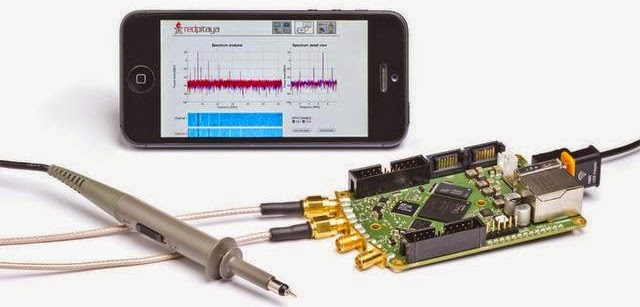
Introducing RED PITAYA - an innovative single board, low cost, high spec, multifunctional and portable PCB based electronic Test & Measurement Device that aims to replace expensive lab and field instruments.

RED PITAYA – Open Source T&M Device

RED PITAYA – Open Source T&M Device

Features
RED PITAYA is a programmable device powered by Xilinx Zynq7000 SoC that combines dual core ARM & FPGA and runs on Linux. It uses open source ecosystem approach which let users to download standard applications from 'Bazaar' and customize these applications at various programming levels and also develop new applications using source code and documentation available from 'Backyard'.

It is an ideal platform for electronic enthusiasts, students and universities, HAM Radio operators and research institutes.


Red Pitaya In Action


Hardware Specifications of Red Pitaya

Inputs:-
1. The main inputs are two independent channels that run at 125MS/s with 14-bit resolution
2. Four low speed inputs, each at 100kS/s and 12-bit resolution.
Outputs:-
1. Two main analogue outputs at 125MS/s and 14-bit.
2. Four low speed outputs, each at 100kS/s and 12-bit resolution.

Expansion is possible via USB (to add a flash drive, WLAN adapter or camera for instance), and also via a connector that provides 16x FPGA pins for GPIO (e.g. for a custom add-on module). The instrument is typically accessed over Ethernet via a web interface and can be easily connected to local networks. Users can connect to it by simply writing its IP in the address bar for their browsers.

It is also possible to log in, execute remote commands and transfer data via SSH. A handy USB UART interface provides access to the SoC serial console for configuration and debugging.

Hardware Specifications of RED Pitaya


Standard Applications/Functionalities

Oscilloscope - 2 channels @ 125 MS/s 14 bit digital with external or signal based triggering capability
Spectrum Analyser - 2 channels with 50 MHz bandwidth signal with waterfall diagram capability
Arbitrary Waveform Generator - 2 channels @ 125 MHz 14 bit arbitrary waveform generation with external triggering capability

Frequency Response Analyser - 2 channels with 60 MHz bandwidth

The web interface enables access to Red Pitaya’s functionality from the majority of browsers. Applications are available on iPhone, iPad, other smartphones, tablets and PCs.

Software Functionalities, Programming
Red Pitaya can be customised for specific applications above its standard specification. It is based on GNU/Linux operating system and can be customised at different programming levels. Available software interfaces include:
- HDL
- C/C++
- Scripting languages
- Matlab
- HTML based web interfaces

Red Pitaya Target Audience
ELECTRONICS ENTHUSIASTS. Red Pitaya is a great springboard for electronics enthusiasts, because it offers great user interface and can be easily reconfigured for any kind of interaction with outside world by simply modifying the available applications. Out-of-the-box applications, such as oscilloscope or spectrum analyzer, enable fast debugging of electronic projects

STUDENTS. The learning process is simplified by Red Pitaya Backyard containing all the application's source code. Students can start programming by applying incremental changes to the code and publish their work in Bazaar and easily get in touch with a wide range of technologies and knowledge. It is also very appropriate for PhD or other research projects

TEACHERS & PROFESSORS. Red Pitaya is a compact replacement for several expensive instruments and also a universal teaching tool. It enables learning of WEB and embedded application programming, FPGA, signal processing, machine vision applications and it can be controlled by Matlab as well.

HAM RADIO OPERATORS. Amateur radio community uses a wide set of instruments such as SWR meter, network analyzer etc. Red Pitaya has a potential to replace them all. Besides that it can also be used as a radio station or software defined radio (SDR)

RESEARCH INSTITUTIONS. Red Pitaya is very suitable solution for detecting and analyzing fast phenomena, as well as generating or simulating complex signals.

To Conclude
RED Pitaya with its out-of-the-box features, applications & high spec caters to the requirements of all electronics professional working in different areas & on different applications that too at a very affordable price. It is not hard to believe that in coming days RED PITAYA with so much of distinguished features can become inseparable/invaluable device for any electronics lab, design house, R&D center, and university.


Sourced By: EFY:


0

Water-Level Indicator Schematic

Here’s a simple water-level indicator for overhead tanks that uses three LEDs (LED1, LED2, and LED3) to indicate minimum, middle, and maximum water levels in the tank.

The sensor probes comprise A, B, C, and D, where A is the common probe and B, C, and D are meant for sensing the minimum, middle, and maximum levels, respectively. When water in the tank touches sensor wires A and B both, a small current passes from A to B through water and to the base of transistor T1 via resistor R1. As a result, transistor T1 conducts, causing LED1 to glow. Similarly, when water touches sensor C, LED2 glows to indicate that the water has reached the middle level. Finally, when water touches sensor D, LED3 glows to indicate the maximum level of water. Thus all the three LEDs glow when the tank is full. At this stage, the motor should be switched off manually.


Water-Level Indicator Schematic


Water-Level Indicator Schematic


The circuit can be easily assembled on a general-purpose PCB and enclosed in a wooden box. The three LEDs should be mounted on the front panel of the box with a spacing of about 4 cm between them. Short lengths of four 18 SWG copper wires may be used for sensor probes. For the common sensor A, a bare copper wire of 18 SWG should be used. For sensors B, C, and D three single-core PVC wires should be used, with their insulation removed to a length of one centimetre towards the ends. All the four wires may be tied around a 12.5mm dia. PVC tube with nylon thread at different heights, without touching each other (not shown in figure).

The sensor probes should be kept in the tank vertically and connected to the main circuit using four flexible PVC wires of different colours.

The circuit is powered by a battery eliminator or a 6V battery and kept near the motor switchboard. The current drawn by the circuit, when all the LEDs glow, is up to 50 mA, which is less than the current drawn by a 6V bed-lamp.

The circuit costs around Rs 50.


Sourced y: EFY Author:  P. Venkata Ratnam


Tuesday, February 17, 2015

0

Simple 6V to 12V Converter Circuit Diagram

 This inverter circuit can provide up to 800mA of 12V power from a 6V supply. For example, you could run 12V car accessories in a 6V (British?) car. The circuit is simple, about 75% efficient and quite useful. By changing just a few components, you can also modify it for different voltages.

Notes

  • L1 is a custom inductor wound with about 80 turns of 0.5mm magnet wire around a toroidal core with a 40mm outside diameter.
  • Different values of D3 can be used to get different output voltages from about 0.6V to around 30V. Note that at higher voltages the circuit might not perform as well and may not produce as much current. You may also need to use a larger C3 for higher voltages and/or higher currents.
  • You can use a larger value for C3 to provide better filtering.
  • The circuit will require about 2A from the 6V supply to provide the full 800mA at 12V.


6V to 12V Converter Circuit Diagram


Simple  6V to 12V Converter Circuit Diagram


Parts
R1, R4 2 2.2K 1/4W Resistor
R2, R3 2 4.7K 1/4W Resistor
R5 1 1K 1/4W Resistor
R6 1 1.5K 1/4W Resistor
R7 1 33K 1/4W Resistor
R8 1 10K 1/4W Resistor
C1,C2 2 0.1uF Ceramic Disc Capacitor
C3 1 470uF 25V Electrolytic Capcitor
D1 1 1N914 Diode
D2 1 1N4004 Diode
D3 1 12V 400mW Zener Diode
Q1, Q2, Q4 3 BC547 NPN Transistor
Q3 1 BD679 NPN Transistor
L1 1 See Notes
MISC 1 Heatsink For Q3, Binding Posts (For Input/Output), Wire, Board


Sourced By:  circuitsdiagram-lab


Thursday, February 5, 2015

0

Brushless DC Motor Driver Circuit Diagram

Use of brushless DC motors (BLDCs) is on the rise. But their control usually requires rotor-position information for selecting the appropriate commutation angle. Normally, a Hall Effect sensor is used to sense rotor position. But in cost-sensitive applications, a sensor-less commutation scheme is often desirable. The circuit described here uses a DRV10866 driver IC to drive a small BLDC fan, without using any position sensors. A BLDC fan’s speed can be varied smoothly, without the usual steps associated with a normal AC fan.

Circuit and working
Fig. 1 shows the circuit of a sensor-less BLDC motor driver. The circuit is built around an NE555 (IC1), a DRV10866 (IC2) and a few other components.


Brushless DC Motor Driver Circuit Diagram

Fig. 1: Circuit of brushless DC motor driver

Fig. 2: An actual-size, single-side PCB for the brushless DC motor driver

Fig. 2: An actual-size, single-side PCB for the brushless DC motor driver
  
Fig. 3: Component layout for the PCB
 Fig. 3: Component layout for the PCB

DRV10866 driver IC from Texas Instruments is used to drive a small three-phase BLDC motor (M1). The circuit is of a three-phase, sensor-less motor driver with integrated power MOSFETs having drive-current capability up to 680mA peak. DRV10866 is specifically designed for low noise and low component-count fan-motor drive applications. A 150° sensor-less back emf scheme is used to control the three-phase motor.


A 100k pull-up resistor (R2) is used at pin 1 of IC2. Pins 2, 4, 7 and 6 of IC2 are connected to common, phase A, phase B and phase C of the BLDC motor, respectively. Pin 10 of IC2 is connected to pin 7 of IC1 to get the pulse-width modulated (PWM) signal from IC1 to control the speed of the BLDC motor.


The output signal (PWM) is available at IC1’s pin 7 (DIS) and not from the usual output pin 3 of the IC. The 25kHz (approx.) PWM signal’s duty cycle can be adjusted from 5% to 95% using potentiometer VR1. The speed of the BLDC motor can be controlled by varying the duty cycle of the PWM signal. Turning VR1 counter-clockwise lowers the duty cycle which, in turn, lowers the speed of the motor, and vice versa.

Construction and testing

An actual-size, single-side PCB for the brushless DC motor driver is shown in Fig. 2 and its component layout in Fig. 3. Assemble the circuit on the recommended PCB to minimise assembly errors. IC2 should be fitted on solder side of the PCB.

After assembling the components, connect a 5V DC supply to CON1 connector. To test the circuit for proper functioning, verify correct 5V supply for the circuit at TP1 with respect to TP0. Turn VR1 clockwise or counter-clockwise to increase or decrease the speed of the motor.


Author Name: Abhijeet Rai Sourced By: EFY


Social Time

Google Plus
Follow Us
Pinterest
Follow Us

Subscribe to our newsletter

(Get fresh updates in your inbox. Unsubscribe at anytime)