Video of the Day

Sunday, January 25, 2015

0

Led Flasher Type of Police Circuit Diagram

This is the simple Led Flasher Type of Police Circuit Diagram. LED flasher same as that used in the police car, where the pace at which the lights flash is well paced and there is a sequence on each side. This type of flasher is also called strobe light or stroboscopic light. I began to develop a project to be published here, but by coincidence I ended up finding a circuit, easy to build and giving effect was wanting.

The electronic circuit flasher police is a Russian site, as the Russians have their own markup for semiconductor like this project, which uses KT815 transistors, for sure you will not find these transistors in a Western store, but of course are the replacements, in this case BD135.

Led Flasher Type of Police Circuit Diagram

Led Flasher Type of Police Circuit Diagram


Flasher LED Police type


This circuit is a classic of electronics, a flip-flop circuit, "astable multivibrators", this circuit is used for common flasher, but in this case two of this circuit were coupled to give the desired effect. The circuit flasher is so simple that can be done by a novice, as we see in the image below of the author, it was made on a standard printed circuit board.

How does the flasher Police

The flasher consists of two astable multivibrators, a leading astable formed by VT1 and VT2 transistors that generate the strobe and VT3 eVT4 transistors that have created short pulses to VT1 and VT2. The master oscillator is switched alternately strobe generator and the operating frequency of the generator is determined by the capacitors C1 and C4 and resistors R5, R6, R8 and R9.

You can use the trimpot R7 and R10 resistors to change the frequency of multivibrators, changing the frequency of blinking of the LEDs. The power transistors VT1 and VT3 and resistors R1 and R2 depend on the power of the LEDs used in the circuit.

Have the circuit power supply can be made with voltages 6-9 V, and its consumption is very low, enabling the use of batteries or battery. You can also change the operating voltage to 12 volts, just change some circuit resistors or put a 7809 regulator in input voltage.

Flasher LED type Police

I will give the most common equivalent found, the VT1 and VT2 transistors can be replaced by medium power transistors BD135, BD137 or BD139. The VT3 transistor can be replaced by transistors average power transistors BD136, BD138 or BD140.

But the transistor VT4 can be replaced by transistor 2sa611, BC556 or 2N4058 and other BCs of life. Below the video of the flasher police, the circuit can also be used for security systems, emergency flashing, holiday lighting, etc.


You can use higher power LEDs in this circuit since modify the resistors R1 and R2.


Friday, January 23, 2015

0

Simple Interface for Digital Sound Synthesis

You can make a digital sound synthesizer, for experimentation with sound equipment or with peripheral devices, using special integrated circuits or digital-to-analogue converters (DACs). But here is a simple 8-input digital sound-synthesis circuit for producing audio from digital codes that can be easily interfaced with microcontroller or microprocessor boards having up to eight TTL/CMOS-level digital output pins.

Circuit and working
Fig. 1 shows circuit diagram of the simple interface for digital sound synthesis. It is built around low-power audio amplifier LM386 (IC1), 9V voltage regulator 7809 (IC2) and a bridge rectifier (BR1).

Simple interface for digital sound synthesis
Fig. 1: Simple interface for digital sound synthesis


The 8-bit digital code (representing audio signal) input is applied at connector CON4. Resistors R1 through R8 and potmeter VR1 work as a simple DAC circuit. The relationships to get approximate values of resistors in the DAC are:

R1 = 2R2 = 4R3 = 8R4 = 16R5 = 32R6 = 64R7 = 128R8
Value of VR1 can be from 10% of R8 to 20% of R8.

The minimum value of each resistor (R1 through R8) depends on digital output levels. Capacitors C14 and C15, with switches S1 and S2 closed, filter the sound signals, and can be omitted, if not needed.


Fig. 2: An actual-size PCB layout for the circuit

The audio input is amplified by LM386 low-power amplifier. The gain is set to 200. With 9V power supply, the circuit outputs around 0.5W. The loudspeaker can be 4-ohm, but 8-ohm or higher is preferred to avoid overloading LM386.

The power supply is built around voltage regulator 7809 which gives a 9V regulated output. You can use 4-9V DC as external supply at CON7 input when 230V AC mains is not available.

Diode D1 is used for reverse protection of the regulator.

Construction and testing
An actual-size, single-side PCB for simple interface for digital sound synthesis (excluding the dotted box shown in the circuit) is shown in Fig. 2 and its component layout in Fig. 3. After assembling the circuit on a PCB, enclose it in a suitable plastic box.


Fig. 3: Component layout for the PCB

For testing, generate 1kHz square-wave signal and connect it to any input line of CON4 (D0 through D7). You will hear sound in the speaker connected at CON5.


You can write a simple software code, burn it into the microcontroller, connect its port pins to CON4 and check output from the speaker. You may change the code to various audio frequencies and check the output for experimentation.


You can also use this circuit as a simple audio signal mixer by applying the audio signals (including square-wave signals) at inputs D0 through D8.

Before using the circuit, do verify that voltages at test points are as per table.
The author was a researcher and assistant professor in Technical University of Sofia (Bulgaria) and expert-lecturer in OFPPT (Casablanca), Kingdom of Morocco. Now he is working as an electronics engineer in the private sector Bulgaria


Share on stumbleupon Share on gmail Share on facebook Share on twitter More Sharing Services


Sourced By:  EFY: Author Petre Tzv Petrov


Thursday, January 15, 2015

0

Tiny DDS - Open source DDS generator Project

This project is an open source (hardware & software) DDS generator, based on: smart TFT module, AD9834, LM7171 fast amplifier.

Description

The homemade function generator is a quite common project on the internet. We can find different ways to do it:

- The quick & dirty way based on a DDS module bought on eBay
- The analog version based on a MAX038 / XR2206
- The “clean” way based on a FPGA and a fast DAC (e.g. http://www.circuitben.net/node/14)
- The software way (e.g. Arduino + R/2R DAC)

From my side, I wanted a small one which could fits my needs without being too expensive. According to me, such generator should at least:

- Be easy to use
- Output a signal from 1Vpp to 10Vpp (+/-5V), from 0 to 1MHz
- Have a low profile
- Without electric hazard (shall work on a 12V DC)


Tiny DDS - Open source DDS generator Project Schematic

Tiny DDS - Open source DDS generator Project

Choosing the DDS chip
I first started to look for a cheap DDS chip on eBay; you have to be careful because most of DDS chips have only a sinusoidal output. Since I also want a triangular output, I have chosen the AD9834. According to its datasheet, this component is able to output a frequency of 37.5MHz from a clock of 75MHz… But do not expect a clean waveform at such frequency: without an internal PLL, this signal would be defined by only 2 points.

From my personal experience, I consider that a waveform shall be defined by 10-20 points to be well restituted. Relying on a 75MHz clock, the maximal output frequency would be 7.5MHz… This is not a very good performance for a professional equipment (even if the cheapest generators do not go above 4MHz), but it is quite reasonable for a hobbyist project.

The AD9834 can be found at $5 on eBay.

Amplitude control

The amplitude of the AD9834 can be controlled through different ways:

- Constant amplitude of 1Vpp (by default on most COTS), by wiring a resistor between the FS_ADJUST pin and the ground: this is quite annoying because an additional external amplifier will be need to set the amplitude to a desired level.

- Variable amplitude, by wiring a potentiometer between the FS_ADJUST pin and the ground: this solution is really easy to implement, but it will not allow a software management needed, for example, by the amplitude modulation.

- Software variable amplitude, by wiring a DAC to the FS_ADJUST pin. This solution is a bit more complex, but it will allow to implement some useful functionalities. I choose this way.

The amplitude will be set by the microcontroller of the smart TFT module (PIC32MX795). Unlike the other manufacturers (Atmel, ST…), Microchip did not include a DAC on their $10 chip… An external DAC is needed (an AD5310 found on eBay for $0.8 – 10 bit / SPI, SOT23-6 package). A small voltage divider is put between the DAC and the FS_ADJUST pin in order to transform the 0-3.3V of the DAC into 0-1.2V handled by the AD9834:


Notice: the logical levels are reversed: the minimal amplitude is reached when the DAC output is 3V3 and the maximal amplitude is reached when the DAC output is 0V.


AC coupling

The AD9834 generates a signal with a non-null offset, variable according to the amplitude. At this point, this offset is very annoying and shall be removed. Two possible ways:

- A high pass filter (a simple RC filter): this solution ensures an ideal AC coupling, but is problematic for the low frequency signals (a huge RC filter would be needed for frequencies below 100Hz)

- A differential amplifier: it is possible with the AD9834 because this component already has a differential output (IOUT / IOUTB pins). This solution makes the AC coupling effective even for very low frequencies, even for a DC signal. Therefore, the AC coupling will not be “ideal”: a small offset will be injected, and possibly some additional distortions due to the tolerance of the components (OPAMP & resistors). Nevertheless, it remains the best way according to me.


The ratio R15/R12 is set such as the maximal voltage outputted by U6 is +/-3.3V.

Offset control

Nothing difficult here: we just have to generate a DC signal between -3.3V and +3.3V. I use another AD5310 with a small OPAMP:


Notice: here again, the logical levels are reversed: the minimal offset is reached when the DAC output is +3.3V and the maximal offset is reached when the DAC output is 0V.

Final stage

Here, we have 2 signals: the one coming from the DDS (between -3.3V and +3.3V, AC coupled) and the one coming from the offset control (between -3.3V and +3.3V too). We just have to mix these 2 signals and amplify them to get a +/-5V output:


The LM7171 is able to output more than 100mA; nevertheless, the current is limited through a 100R resistor. A small LC filter is also implemented before the main output for filtering the 75MHz clock residual.

PWM output

Nothing complex here: a simple CMOS gate for buffering the PWM output of the microcontroller. I tried to use a fast comparator on the triangular output of the DDS, but the jitter was too important; I finally gave up this solution.


Analog input

Very minimalist… A simple resistor for limiting the input current, and a common Pi filter. The sampling frequency is not very high (~ 1KHz) because the internal ADC of the microcontroller is also used by the touchscreen inside an ISR.


Power supply / regulators

The generator is powered by a standard 12V plug. Some switching regulators produce the 5V (for the smart TFT module) and the +/-7V (used by the analog stage). The 3.3V comes directly from the smart TFT. The LT1616 are an expensive components on Farnell, but I found these on eBay for $0.8. Notice that any buck regulator should do the job here (+5V@200mA, +/-7V@200mA).

PCB

The whole schematic can be easily routed in a small PCB (smaller than a credit card). The PCB is composed of 2 layouts, with a common GND plan. The LM7171 shall be routed with care: due to its topology (fast OPAMP – 400MHz), a bad layout will make it oscillate. For this reason, I also add a footprint for a small 1pF capacitor: if the layout is not correct, I should be able to limit the oscillations with it.


Assembling the board

The PCBs (from SeeedFusion):


The finished board:


Assembled with the smart TFT:


Software

After a first quick & dirty attempt, I had to enhance the interface look; this one is working properly, but I admit that the old win95 look is really outdated. Moreover, there is a flickering issue on some widgets which are highly solicited (e.g. the frequency valueBox). The new interface is based on a brushed metal background, with dark widgets. I have also implemented the double buffering for the concerned widgets:


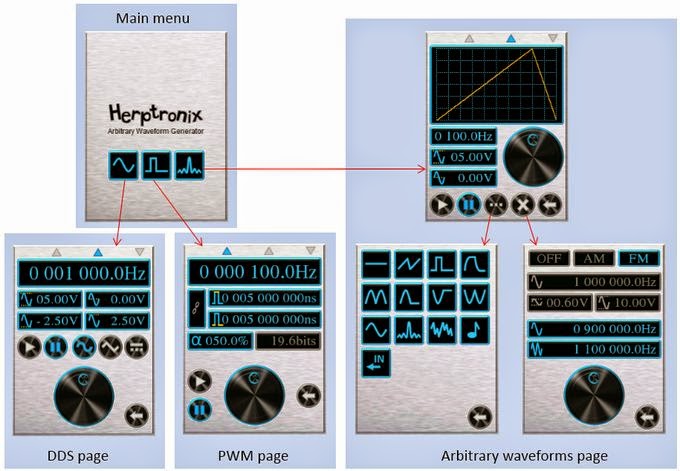
The new look is more modern (according to me; I’m not a graphic artist :s). The interface is still very reactive, but the memory footprint literally explodes (more than 90% of the flash memory is used). The user interface is composed of 4 “pages”:

- DDS (sinus/triangle waveform, with frequency / amplitude / offset control)
- PWM (PWM signal only)
- ARB (arbitrary waveforms & modulations)
- A menu page


Sinus / triangle waveform generation

These waveforms are directly generated by the AD9834, just by configuring its internal registers through the SPI bus. Nevertheless, a small detail shall be handled by the program: the frequency register is coded on 28 bits, split on two 16 bits registers. The access to the frequency register is not an atomic operation and shall be buffered first (through the FREQ0 / FREQ1 registers).

Arbitrary waveforms generation

I use the internal DAC of the AD9834 to generate these signals: this solution allows to keep the whole analog stage as is (same amplitude / offset control). For using the internal DAC, I configure the AD9834 with a triangle signal of 0Hz; then, I set the phase register to obtain the desired output voltage.

Some basic waveforms are available, such as saw tooth, exponential, noise, sin(x)/x… It is also possible to draw a waveform and play a wav file. However, there is a bandwidth issue: the AD9834 is accessed through a SPI bus, and even with a 20MHz clock, several microseconds are needed to send a single sample on the output. At the end, the microcontroller cannot provide more than 100kSPS (kilo Sample Per Second). Above this rate, the program is ran very slowly (most of the CPU time is spent into the ISR).

Go further

Even if this generator works properly, I have to admit that its electrical characteristics are closer to a gadget than a professional equipment (SNR below 45db). However, it would be easy to enhance its performances by modifying some components:

The DDS chip

A DDS such as the AD9102 is much more powerful than the AD9834; besides its more accurate DAC (14bits vs 10bits), its internal LUT can be reprogrammed: where the PIC32 can only provide 100kSPS, the AD9102 can provide up to 180MSPS (1800 time more). Unfortunately, this device is more expensive ($15/u at 100u) and is available only in LFCSP package (quite hard to solder).

The analog stage

The power supply should be changed first: the +/-7V coming from the buck regulators are obviously problematic (the output signal has some noise – 1.5MHz @10mVpp). A simple power supply based on a toroidal transformer and some 78xx / 79xx would be better. The LM7171 OPAMPs should also be changed by a more appropriate chip (a current feedback OPAMP for example).

DAC

The 10 bits of the AD5310 might not be the wisest solution for this application: for 10Vpp, 1LSB is equivalent to ~10mV, which is pretty good… if you use the whole range of the DAC! I reduced the range from 0-1023 to 0-920 due to the tolerance of the components, leading to an 11mV/LSB resolution. A 12 bits DAC would be a better solution here, thus a true voltage reference (the current one is derived from the 3.3V supply).[Link] Author: Philippe Duboisset


Sunday, January 11, 2015

0

Versatile Audio-Visual Alarm Circuit Diagram

This circuit uses an NE555 timer IC, some LEDs, a couple of piezo buzzers and a few other components to produce audio-visual effects as per your requirement. The timer NE555 and its equivalents are widely used for all sorts of audio and visual indications, such as door alarms. But the sound produced by these circuits may not be always pleasant to hear, or the light produced may not be visually appealing. With this circuit you can get different audio-visual effects.

Here we use LEDs for visual indication and buzzers for audible alarms as they require relatively low current to operate. By simply connecting some resistors and capacitors to NE555 we can obtain some interesting visual and audible effects as described here.

Circuit and working
Fig. 1 shows the circuit of the versatile audio-visual alarm which is built around timer NE555 (IC1), LEDs, buzzers and some resistors and capacitors. Resistors R1 and R2 and capacitor C1 determine the frequency of the LEDs’ blinking. The frequency is selected usually within the range of 0.1Hz to 20Hz, depending on your requirement. Values of resistors R1 and R2 can be above 1-kilo-ohm. Capacitor C1’s value can be between 1µF and 1000µF.

Versatile Audio-Visual Alarm Circuit Diagram

Fig. 1: The versatile audio-visual alarm circuit


Fig. 2: Actual-size, single-side PCB for the circuit

 Fig. 3: Component layout for the PCB


Timer NE555 drives two outputs, namely, Group1 and Group2. Group1 is built around resistors R4 and R6 along with LED1 through LED6. Group2 is built around resistors R7 and R8 along with LED7 through LED12.


Each of the groups can be configured to get different outputs. For example, in Group1 you can use only the LEDs (LED1 through LED3) connected to +12V, or only the LEDs (LED4 through LED6) connected to the ground, or both branches of these LEDs, or only piezo buzzer PZ1, or PZ1 with any combination of the LEDs, or you can omit the entire Group1.

The components in Group2 can form the same combinations as the components in Group1. The difference between the Group1 and Group2 is the use of resistor R5 and capacitor C2. These two components give light-decay effect to the LEDs and a pleasant low-pitch sound to piezo buzzer in Group2. Value of resistor R5 can be between 75-ohm and 1-kilo-ohm and that of capacitor C2 between 47µF and 1000µF.

At point 1 (TP2) in the circuit you can see a rectangular wave signal. At point 2 you can see a triangular or trapezoidal-like signal. The signals at points 1 and 2 should go low, almost to zero, and should go high, almost to 12V supply voltage.

Power supply used is 12V, but it can be in the range of 4.5V to 15V as well, depending on the number of LEDs used in each branch. Higher number of LEDs will require higher voltage. LED13 glows when power supply is connected in the circuit.

Resistors R4, R6, R7 and R8 are selected according to the number and type of the LEDs used. If the values of these resistors are too low, the output of the timer will be overloaded and the LEDs in the upper and the lower branches will get activated simultaneously.


Overloading may also damage the NE555 timer. It is suggested to keep the total output current drawn from NE555 below 100mA.

On/off switch S1 is used to start or stop the alarm. Connector CON2 is an optional input point for connecting a variable element, such as a preset, for adjusting or varying the frequency of the square signal for more audio-visual effects.

Construction and testing
An actual-size, single-side PCB for the versatile audio-visual alarm is shown in Fig. 2 and its component layout in Fig. 3. After assembling the circuit on PCB, enclose it in a suitable plastic box.

Connect piezo buzzers PZ1 and PZ2 at their provided places in the PCB. Also connect 2-pin terminal CON1 for power supply. Connect CON2 for external input (optional). Before using the alarm circuit, check at the test points given in the table.


Saturday, January 10, 2015

0

300mA DC to AC converter Circuit Diagram

This is the Simple 300mA DC to AC converter Circuit Diagram. This circuit was used to provide battery backup to a device that had an AC (output)wall transformer. Due to the quasi sine-wave output and imprecise 60Hz output frequency, some devices might not work pro perly. Peak output is the DC input voltage minus about 20 ohms drop. Use bigger output MOSFETS for more current output.[link]


 Simple 300mA DC to AC converter Circuit Diagram


Simple 300mA DC to AC converter Circuit Diagram


Monday, January 5, 2015

0

Temperature warning indicator circuit

The circuit is a low temperature regulator, supervisor, warns us about global warming. Temperature control is done by the thermistor TH1, which is a negative factor. The resistance varies between 10KO at 25 ° C and about 1KO at 94 ° C. The trimmer TR1 regulate the exact temperature at which the Q1-2, connected as a Darlington, lead me, making the relay K1 to close and IZ, sound.

The alarm is activated when the temperature is greater than the default. The thermistor should be located away from the rest of the circuit, so as not to risk from the heat. The power circuit is battery 9V, but if it is mounted in a fixed position, then we can supply with a constant voltage power supply. The relay contacts can be connected load which we, as a bulb, another circuit, etc. It can also add an LED, if we are to sign and visual stimulation.

The adjustment is done by immersing the thermistor TH1, in the water which we know the temperature (contacts should be well insulated so we do not have short circuit) and adjusting the trimmer until the circuit is excited. The cable connecting the circuit with the TH1 must be shielded.


Temperature warning indicator circuit


Temperature warning indicator circuit


Part List
R1= 820 ohm
R2-3= 1Kohm
C1= 220uF 16V
TR1= 2.2Kohm Trimmer D1= 5.6V 0.5W Zener
D2-3= 1N4148
Q1-2= BC550C
TH1= Thermistor 10Kohm at 25° C
 K1= 6V 200 ohm Relay
BZ1= Buzzer
S1= 1×2 Switch
BATT= Battery 9V or external supply
Application
This circuit is designed not only setting a detection of high temperatures, but can also be changed to be set on the detection of low temperatures in some areas. It can be used for refrigeration, walk-in refrigerator or freezer and other environments that are sensitive to temperature. Some integrated circuits high-temperature alarm modules will be used in motor vehicles to the profession in which the temperature element senses a temperature very dangerous in the interior of a motor vehicle, and encourages the employment sensor detects the presence or determine the absence of an occupant. In the absence of the inhabitants, the sensor is that after a period during which an audible alarm is activated to provide the attention to the motor vehicle in the presence of an occupant. This type of alarm can be reset with a key.
Take a temperature alarm can be advantages such as protection of valuable equipment by high temperature, low temperature, high humidity or sometimes provided. Other programs of high temperature can be used to protect against loss of or against the air conditioning system for heating off. Instead, the program for low-temperature failure of the heating system be used to prevent frozen pipes. The alarm can also reduce downtime, get a phone call and the notification of a possible power failure or failure before damage occurs in one unit. [Link]


Sunday, January 4, 2015

0

Automatic Evening Lamp Circuit Diagram

Presented here is a solution for switching off outdoor lamps even when you are not at home. The lamp turns on in the evening and turns off in the morning so that there is no need for manually switching it on/off. The circuit is directly powered from AC mains and can be enclosed in a plug-in type adaptor box. It can drive a bulb, CFL, tubelight, LED lamp, etc up to 200W. Author’s prototype is shown in Fig. 1.

Circuit and working

Author’s prototype
Fig. 1: Author’s prototype

The circuit uses a transformer-less power supply to generate low-volt DC. As capacitors C1 and C2 are connected in AC lines, these should be X-rated capacitors. This minimises space and makes the unit light-weight. Unlike an ordinary capacitive power supply, a more efficient power supply design is used for spike-free operation. Phase (L) and neutral (N) lines have identical circuits so reversal in polarity while plugging will not affect the circuit. 105K (1µF) 400V AC capacitors are used that can drop 230V AC to low-level AC. Resistors R1 and R2 protect the power supply from instant inrush current. Bleeder resistors R3 and R4, parallel to C1 and C2, remove the stored current from the capacitors at power off to prevent shock from stored energy in the capacitors.

A full-wave rectifier bridge comprising D1 through D4 (1N4007) rectifies low-volt AC to DC and smoothing capacitor C3 gives ripple-free DC for the circuit. The output voltage from the power supply is sufficient to operate the circuit including the relay. Green LED1 indicates power-on status. Resistor R5 limits LED current.

Automatic Evening Lamp Circuit Diagram
Fig. 2: Circuit diagram of an automatic evening lamp

The circuit is a simple bi-stable arrangement using popular timer IC 555 (IC1). Linking its threshold (pin 6) and trigger (pin 2) controls its flip-flop operation. When the threshold input is high, it resets the flip-flop and keeps the output low. When the trigger input is low, flip-flop triggers and output turns high. So the combined action of threshold and trigger inputs gives the bi-stable switching action to control relay driver transistor T1. The bi-stable action of IC1 is controlled by LDR1 and resistor R6 (470k). The value of 5mm LDR can be up to 1 mega-ohm, depending on the ambient light conditions. A 1MΩ variable resistor in place of R6 can make the sensitivity adjustment easy.

During day time, LDR1 has low resistance, which makes threshold pin 6 of IC1 high. This resets the timer and the output of IC1 remains low. It takes transistor T1 to cut-off state. The relay is de-energised, so the lamp remains off during day time.

Actual-size PCB layout of an automatic evening lamp

Fig. 3: Actual-size PCB layout of an automatic evening lamp

Component layout of the PCB
Fig. 4: Component layout of the PCB

When the intensity of sunlight reduces in the evening, LDR1 offers more resistance and the current through it ceases. This makes both threshold and trigger inputs of IC1 low and the timer changes its output to high. Transistor T1 is switched on due to saturation action. The relay is energised, contact change-over takes place and line is extended to bulb B1. As the circuit is complete, the bulb will be switched on. It will remain lit throughout the night.


In the morning, the situation will get reversed; threshold pin 6 and trigger pin 2 go high, timer reverses its output. Transistor T1 goes into cut-off region. The relay will be de-energised and the bulb will get switched off.

Capacitor C5 at the base of transistor T1 gives a slight lag during on/off of T1 for the clean operation of the relay. Freewheeling diode D5 eliminates back EMF from the relay coil and protects T1 during its switch off. Red LED2 indicates the actuation of the relay.

Construction and testing
An actual-size, single-side PCB layout for the automatic evening lamp is shown in Fig. 3 and its component layout in Fig. 4. After assembling the circuit on a PCB, enclose it in a suitable plastic case.

Give sufficient spacing between the power supply section and the remaining circuit. Provide holes on the front side of the enclosure for LEDs and LDR. Connect phase line (L) to the common contacts of the relay and neutral line (N) for the bulb to the N/O (normally open) contacts of the relay. A 5V PCB relay is used. Ratings of the relay must match with the load. Since the circuit is directly powered from high-volt AC, extreme care is necessary during testing.

First assemble the power supply section up to green LED and connect to AC lines. If the green LED turns on, power supply section is alright. After disconnecting the circuit from mains, assemble the circuit around IC1. Test this part using a 9V battery connected across capacitor C3. If relay RL1 energises after masking LDR1, the bi-stable section is working.

Now the relay connections can be done. Keep the unit outdoor in a place where sufficient light is available. Light from the lamp should not fall on LDR1.

Caution. Since this circuit has mains voltage on board, extreme precautions need to be taken. Do not troubleshoot when it is connected to the mains. Test only after taking adequate precautions to prevent shock hazards.


Sourced By: EFY: Author:  D. Mohan Kumar


Thursday, January 1, 2015

0

Build 20W MOSFET Power Amplifier Circuit with IFR9520,IFR520

As we are like to show you about audio and sound circuit ,I found the circuit which is good one for power amplifier with one MOSFET.

The output power of an operational amplifier is often increased by a complementary emiter follower.

It can also be done with a MOSFET,but it is not a good idea to connect such a device as a complementary souce follower because the maximum output voltage of the opamp is then reduced appreciably by the gate-source control voltage of the MOSFET ,which can be a couple of volts.

20W MOSFET Power Amplifier Circuit with IFR9520,IFR520

Build 20W MOSFET Power Amplifier Circuit with IFR9520,IFR520
20W power amp MOSFET


Another approach is to connect two MOSFETs as a complementary drain follower.The (alternating) output current provided by the MOSFETs is limited by the level of the supply voltages and the saturateion voltages of T3 and T4 Resistor R8,together with R9,provides feedback for both the opamp and MOSFETs .

The open-loop amplification of the opampis,therefore,increased by (1+R8/R9).the closed-loop amplification of the complete amplifier is (1+R3/R2).

The current source formed by T1 and T2 is required for arreanging the quiescent current of T3 and T4 at 50 mA.The values of resistors R4 and R5 are such that,without the current source the voltage drop across the resistor resulting from the direct current through the opamp is not sufficient to switch on T3 and T4 .with the current source,and depending on the setting of P1,the voltages across R4 and R5 rise,which increases the quiescent current through T3 and T4.

In view of the temperature dependence of the quiescent current,T2 must be mounted on the common heat sink(c. 5 K/W) of the MOSFETs.

The output power is not less than 20 W into 8 ohm,at which level the harmonic distortion amounts to 0.075 per cent at 100 Hz to 0,135 per cent at 10 kHz.[link]


0

100 Watt Power Amplifier Circuit With IC TDA7294

Power Amplifier TDA7294 is a power amplifier with IC Power Amplifier is a mono 100W Class AB operation of OCL.

The power supply circuit. Positive, negative, and ground. Usually, we use the power supply circuit to + /-25V to + /-35V at 100W RMS will be used to heat sufficiently.

After many members have already made the TDA7294 as I know, with a sound quality that is the very gods or Hi-End itself.


100 Watt Power Amplifier Circuit With IC TDA7294


100 Watt Power Amplifier Circuit With IC TDA7294


Several days before the member’s PM to me saying that I had an amplifier using IC TDA7294 to have more of the same. Higher power. And low heat.

Achieved by increasing the voltage raising circuit For the more, it means high power and high heat up. Today I have come across. I use IC TDA7294 circuit at the time.

In-Home Use amplifier circuit is a Class G amplifier with low power consumption, resulting in the loss of a 20V DC power less.

And when you’re driving a high-power random access is party to a rhythm. Principles to do it. I took out a membership you can do is try to build up a bit.[link]

We provides PCB both top and bottom side for you.


Social Time

Google Plus
Follow Us
Pinterest
Follow Us

Subscribe to our newsletter

(Get fresh updates in your inbox. Unsubscribe at anytime)